


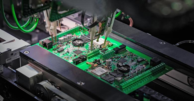
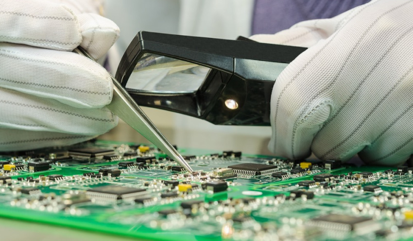
Managing heat in electronic devices is a critical aspect of modern circuit board design. As components become more powerful and densely packed, effective thermal management ensures reliability and performance. One of the most effective tools for dissipating heat in printed circuit boards (PCBs) is the use of thermal vias. This article provides a comprehensive overview of how these specialized vias function, their design considerations, and why they are essential for electronics manufacturing.
Understanding the role of thermal vias is especially important for engineers and product designers aiming to optimize device longevity and efficiency. For those interested in a broader perspective on circuit board materials, the electronic product design pcb material selection guide offers additional insights into choosing the right substrates for thermal performance.
What Are Thermal Vias and Why Are They Used?
In the context of PCB design, a via is a small hole drilled through the board and plated with conductive material, typically copper. While standard vias are used to route electrical signals between layers, thermal vias are specifically designed to transfer heat from hot components to other areas of the board, such as ground planes or dedicated heat sinks.
The primary function of these vias is to create a low-resistance thermal path, allowing heat to move away from sensitive components. This is especially important in high-power applications, such as LED lighting, power supplies, and RF modules, where excessive heat can degrade performance or cause failure.
How Heat Dissipation Works in PCBs
Electronic components generate heat during operation. If this heat is not efficiently removed, it can accumulate and raise the temperature of the device, potentially leading to malfunction or reduced lifespan. Thermal vias act as vertical heat conduits, channeling thermal energy from the component side of the PCB to the opposite side or to internal copper planes.
The effectiveness of these vias depends on several factors:
- Via diameter: Larger vias can transfer more heat but may take up more board space.
- Via count and density: More vias in a given area increase the total thermal conductivity.
- Copper plating thickness: Thicker plating improves heat transfer.
- Connection to copper planes: Direct connection to large copper areas helps spread heat efficiently.
For a detailed look at the overall electronics manufacturing process, including thermal management strategies, see this comprehensive overview of the electronics manufacturing process.
Design Considerations for Effective Thermal Vias
When integrating thermal vias into a PCB, several design choices impact their performance. Here are some key considerations:
Optimal Placement and Array Patterns
Placing vias directly beneath heat-generating components, such as power transistors or integrated circuits, maximizes heat transfer. Often, designers use an array or grid of vias under the thermal pad of a component. The spacing between vias should balance thermal performance with manufacturability, as too many closely spaced vias can complicate soldering and assembly.
Via Filling and Capping Techniques
Vias can be left open (tented), filled with conductive or non-conductive materials, or capped with copper. Filled and capped vias prevent solder wicking during assembly and can improve mechanical strength. Conductive fill materials further enhance heat transfer, though they add to manufacturing cost.
Balancing Electrical and Thermal Needs
While the main role of these vias is thermal, they may also serve as electrical connections to ground or power planes. Designers must ensure that the via pattern does not interfere with signal integrity or create unintended current paths.
Benefits and Limitations of Using Thermal Vias
Employing thermal vias in PCB layouts offers several advantages:
- Improved heat dissipation: Reduces the risk of overheating sensitive components.
- Enhanced reliability: Maintains device performance over time by preventing thermal stress.
- Cost-effective: Compared to external heat sinks, vias offer a low-cost solution for moderate thermal challenges.
- Design flexibility: Can be tailored to specific thermal requirements and board layouts.
However, there are some limitations to consider:
- Manufacturing complexity: High-density via arrays can increase production difficulty and cost.
- Potential for solder wicking: Open vias under pads may draw solder away during assembly, leading to poor connections.
- Limited capacity: For extremely high-power applications, vias alone may not provide sufficient cooling and must be used alongside other methods.
Applications in Modern Electronics
The use of thermal vias is widespread in industries such as automotive, telecommunications, and consumer electronics. They are especially prevalent in devices where compact size and high power density are required, such as LED modules, power converters, and RF amplifiers.
In combination with other thermal management techniques—like heat sinks, thermal pads, and advanced PCB materials—these vias help ensure that products meet stringent reliability and safety standards. For those developing new products, considering thermal management early in the design process is crucial. Further reading on related topics can be found in the electronic product design performance testing guide.
Best Practices for Implementing Thermal Vias
To maximize the effectiveness of thermal vias, engineers should follow established best practices:
- Use a sufficient number of vias under heat sources, but avoid excessive density that complicates assembly.
- Select appropriate via sizes based on available board space and required thermal performance.
- Connect vias to large copper pours or planes to spread heat efficiently.
- Consider via filling or capping to prevent solder issues during reflow.
- Work closely with PCB manufacturers to ensure the design is manufacturable and cost-effective.
Frequently Asked Questions
How do thermal vias differ from standard signal vias?
While both types of vias are holes plated with copper, thermal vias are specifically intended to conduct heat rather than electrical signals. They are usually placed in arrays under hot components and connected to copper planes for optimal heat transfer.
Can thermal vias be used in all types of PCBs?
Yes, they can be incorporated into most PCB types, including single-sided, double-sided, and multilayer boards. However, their effectiveness and implementation methods may vary depending on the board’s thickness, layer count, and intended application.
What are the main challenges when designing with thermal vias?
The main challenges include balancing thermal performance with manufacturability, preventing solder wicking during assembly, and ensuring that the via pattern does not interfere with electrical signals or mechanical strength.
For those interested in additional design considerations, the electronic product mechanical integration guide provides further guidance on integrating thermal and mechanical solutions in electronic products.