

As electronic devices continue to evolve, the demand for faster data transmission and higher processing speeds has made high speed circuit design basics an essential area of expertise for engineers and product developers. Whether you’re working on consumer electronics, industrial automation, or communication systems, understanding the foundational principles behind rapid signal transmission is crucial for achieving reliable and efficient performance.
This article explores the core concepts, common challenges, and best practices for designing circuits that operate at high frequencies. You’ll find practical advice, visual examples, and links to further resources to help you navigate the complexities of modern electronic design. For those interested in related topics, the electronic product design performance testing guide offers valuable insights into verifying and optimizing your designs.
Understanding the Fundamentals of High-Speed Signal Design
At its core, high speed circuit design basics revolve around managing signals that switch or propagate at frequencies where traditional circuit assumptions no longer hold. In these regimes, factors such as signal integrity, electromagnetic interference (EMI), and timing become critical. The transition from low-frequency to high-frequency operation introduces new phenomena, including:
- Signal reflections due to impedance mismatches
- Crosstalk between adjacent traces or components
- Propagation delay and timing skew
- Increased susceptibility to noise and EMI
Designers must account for these effects to ensure that data is transmitted accurately and reliably across the circuit board.
Key Principles for Effective High-Speed PCB Layout
Printed circuit board (PCB) layout is a cornerstone of high-frequency design. The physical arrangement of traces, components, and layers directly impacts signal quality. Here are some essential guidelines:
- Minimize trace lengths to reduce signal delay and reflections.
- Maintain consistent impedance by controlling trace width and spacing, especially for differential pairs.
- Use ground planes to provide a low-inductance return path and shield sensitive signals.
- Avoid sharp corners in traces, as these can cause impedance discontinuities.
- Isolate high-speed signals from analog or low-frequency sections to prevent interference.
For a deeper dive into material considerations, the electronic product design pcb material selection resource explains how substrate choices affect high-frequency performance.
Managing Signal Integrity in High-Frequency Circuits
One of the most significant challenges in high speed circuit design basics is preserving signal integrity. As frequencies increase, even small discontinuities or layout errors can cause data corruption or system instability. Key strategies include:
- Impedance matching: Ensure that the source, transmission line, and load all have similar impedance to minimize reflections.
- Termination techniques: Use series or parallel termination resistors to absorb reflected energy and dampen ringing.
- Controlled rise/fall times: Avoid excessively fast signal transitions, which can generate unwanted harmonics and EMI.
- Proper decoupling: Place capacitors close to power pins to suppress voltage fluctuations and noise.
Simulation tools can help predict and mitigate signal integrity issues before fabrication, saving time and reducing costly rework.
Common Pitfalls and How to Avoid Them
Even experienced engineers can encounter setbacks when working with high-frequency circuits. Some frequent mistakes include:
- Neglecting the effects of parasitic capacitance and inductance, which can distort signals.
- Overlooking return path discontinuities, leading to increased EMI and ground bounce.
- Improper component placement, resulting in long or convoluted signal paths.
- Ignoring thermal management, which can degrade performance or damage components.
To minimize these risks, always review your layout for potential issues, use simulation tools, and consult with colleagues or experts when in doubt. For a broader perspective on the product development process, consider reading about electronic product lifecycle cost analysis to understand how design decisions impact long-term costs.
Best Practices for Prototyping and Validation
After completing your initial design, thorough prototyping and validation are essential. Key steps include:
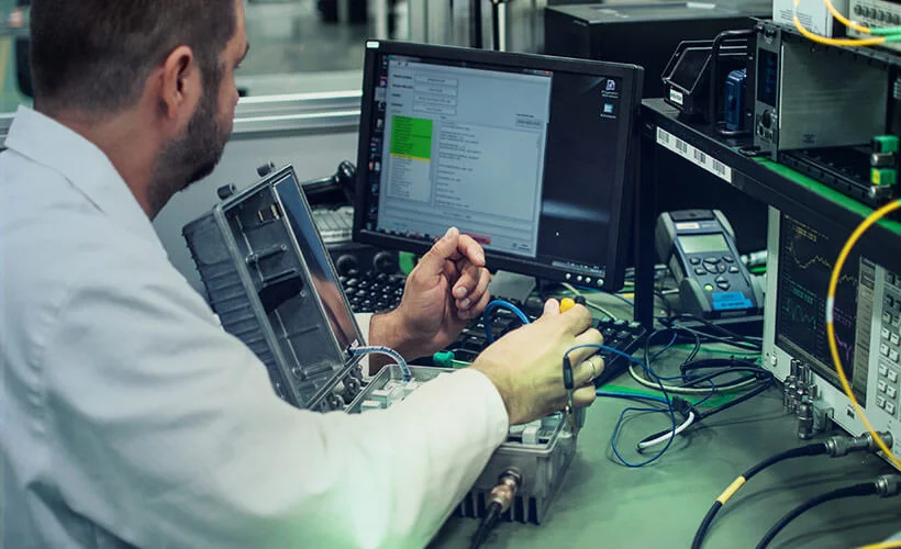
- Build test boards to evaluate signal paths, impedance, and EMI in real-world conditions.
- Use high-bandwidth oscilloscopes and network analyzers to measure signal integrity and timing.
- Perform environmental testing to assess performance under temperature, humidity, and vibration stress.
- Document all findings and iterate on the design as needed.
Validation not only ensures that your circuit meets specifications but also helps identify potential weaknesses before mass production. For more on integrating electronics with mechanical systems, see the electronic product mechanical integration guide.
Industry Resources and Further Learning
Staying updated with the latest trends and techniques in high-frequency design is vital. Many organizations and engineering firms offer resources, training, and consulting. For example, professional design and engineering services for high-speed circuits can provide expert support for complex projects or when scaling up to production.
Additionally, technical forums, webinars, and industry publications are excellent places to learn from peers and stay informed about new tools and standards.
Frequently Asked Questions
What is considered a high-speed signal in circuit design?
Generally, a signal is considered high-speed when its frequency or edge rate is high enough that transmission line effects, reflections, and crosstalk become significant. This often starts at frequencies above 50 MHz or with rise/fall times below a few nanoseconds, but the exact threshold depends on the application and PCB layout.
How can I reduce electromagnetic interference in high-frequency circuits?
To minimize EMI, use continuous ground planes, shield sensitive traces, keep high-speed signals short, and separate analog and digital sections. Proper termination and controlled impedance also help reduce unwanted emissions.
Why is impedance matching important in fast signal design?
Impedance matching ensures that signals are transmitted without reflections or loss of integrity. Mismatched impedance can cause signal distortion, data errors, and increased EMI, especially at high frequencies where transmission line effects dominate.
Conclusion
Mastering high speed circuit design basics is essential for anyone developing modern electronic products. By understanding the unique challenges of high-frequency signals, applying sound PCB layout techniques, and validating your designs thoroughly, you can achieve robust, reliable, and high-performance results. Continue exploring related topics and leverage industry resources to keep your skills sharp and your projects on track.