


Understanding electronics stencil design basics is essential for anyone involved in printed circuit board (PCB) assembly and surface mount technology (SMT). Stencils play a pivotal role in ensuring precise solder paste application, which directly impacts the quality and reliability of electronic products. Whether you are a design engineer, manufacturing specialist, or simply interested in electronics production, mastering the fundamentals of stencil design can help reduce defects, improve yields, and streamline the assembly process.
Before diving into the technical aspects, it’s worth noting that stencil design is closely linked to other aspects of electronic product development, such as electronic product design performance testing guide. Integrating good stencil practices with robust testing and material selection ensures optimal results throughout the product lifecycle.
Why Stencil Design Matters in Electronics Manufacturing
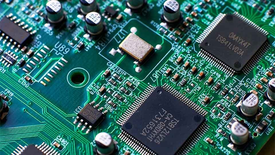
In the context of electronics assembly, a stencil is a thin sheet—typically made of stainless steel or nickel—with laser-cut apertures that align with the pads on a PCB. Its primary function is to accurately deposit solder paste onto the board before component placement. Proper stencil design ensures that the right amount of paste is applied to each pad, which is critical for reliable solder joints and minimizing defects such as bridging, tombstoning, or insufficient solder.
The importance of stencil design extends beyond just paste application. It affects manufacturing efficiency, rework rates, and the overall performance of the assembled product. For those interested in a broader view of electronics manufacturing, resources like this semiconductor fabrication process guide provide valuable context on how stencils fit into the larger production ecosystem.

Key Elements of Stencil Design for PCB Assembly
Several factors influence the effectiveness of a stencil in electronics production. Here are the most important considerations:
- Material Selection: Most stencils are made from stainless steel due to its durability and precision. Nickel and polymer stencils are also used for specific applications.
- Thickness: The thickness of the stencil determines the volume of solder paste deposited. Typical thicknesses range from 0.1 mm to 0.2 mm, depending on component size and pad layout.
- Aperture Design: The shape and size of each aperture must match the corresponding PCB pad. Adjustments such as corner rounding and area ratio calculations help control paste release and minimize defects.
- Surface Finish: Electropolished or nano-coated stencils enhance paste release and reduce cleaning frequency.
- Alignment and Fiducials: Accurate alignment features ensure the stencil matches the PCB layout, preventing misprints and bridging.
Each of these elements contributes to the overall quality and repeatability of the solder paste printing process. For more in-depth guidance on related topics, such as selecting the right PCB materials, refer to the electronic product design pcb material selection resource.
Optimizing Stencil Aperture Design
The heart of any stencil is its aperture pattern. Optimizing aperture design is crucial for achieving consistent solder paste deposits. Here are some best practices:
- Area Ratio: This is the ratio of the aperture opening area to the aperture wall area. An area ratio above 0.66 is generally recommended for reliable paste release.
- Aspect Ratio: The ratio of aperture width to stencil thickness. Maintaining a suitable aspect ratio prevents clogging and incomplete paste transfer.
- Customized Shapes: Modifying aperture shapes (e.g., home plate, rounded corners) helps control solder volume and reduces the risk of defects like tombstoning.
- Reducing Bridging: For fine-pitch components, reducing aperture width or using step-down stencils can help prevent solder bridging between adjacent pads.
These design choices should be tailored to the specific components and layout of each PCB. Collaboration between design engineers and manufacturing teams is key to achieving optimal results.
Common Challenges and Solutions in Solder Paste Printing
Even with well-designed stencils, challenges can arise during the solder paste printing process. Some of the most frequent issues include:
- Insufficient Solder: Often caused by clogged apertures or incorrect stencil thickness. Regular cleaning and proper aperture sizing help address this.
- Excess Solder: Oversized apertures or excessive stencil thickness can lead to bridging and shorts. Adjusting aperture dimensions and using step stencils can mitigate this.
- Paste Smearing: Poor stencil-to-board contact or excessive squeegee pressure can cause smearing. Ensuring flatness and proper pressure settings is essential.
- Misalignment: Inaccurate placement of the stencil relative to the PCB can result in misplaced paste deposits. Using fiducials and alignment systems reduces this risk.
Addressing these challenges requires a combination of good design practices, process control, and regular maintenance. For those involved in the full product lifecycle, exploring topics like electronic product lifecycle cost analysis can provide additional insights into optimizing manufacturing efficiency and cost.
Integrating Stencil Design with the Electronics Manufacturing Process
Stencil design does not exist in isolation. It must be integrated with other aspects of electronics manufacturing, such as component selection, PCB layout, and assembly processes. Effective communication between design, engineering, and production teams ensures that stencil specifications align with the overall goals for product quality and manufacturability.
Additionally, considering regional manufacturing requirements and localization needs can influence stencil and PCB design. For more on this, see the electronic product localization considerations article.
Best Practices for Reliable Solder Paste Deposition
To achieve consistent and reliable solder paste printing, follow these best practices:
- Choose the Right Stencil Thickness: Match stencil thickness to component pitch and pad size for optimal paste volume.
- Optimize Aperture Geometry: Use recommended area and aspect ratios, and customize shapes for challenging components.
- Maintain Cleanliness: Regularly clean stencils to prevent clogging and ensure consistent paste transfer.
- Monitor Process Parameters: Control squeegee speed, pressure, and angle for uniform paste deposition.
- Verify Alignment: Use fiducials and vision systems to ensure accurate stencil-to-board registration.
Implementing these practices can significantly reduce defects and improve the overall quality of assembled electronics.
Frequently Asked Questions
What is the ideal stencil thickness for fine-pitch components?
For fine-pitch components, a stencil thickness between 0.1 mm and 0.13 mm is typically recommended. This range allows for precise solder paste deposition without risking bridging or insufficient solder. The exact value should be determined based on component specifications and pad layout.
How do I prevent solder bridging during assembly?
To minimize solder bridging, ensure that aperture sizes are correctly calculated, especially for closely spaced pads. Reducing aperture width, using step-down stencils, and optimizing paste volume are effective strategies. Regular stencil cleaning and accurate alignment also play a crucial role.
Why is area ratio important in stencil design?
The area ratio affects how well solder paste is released from the stencil aperture onto the PCB pad. A higher area ratio (above 0.66) ensures reliable paste transfer, reducing the risk of insufficient solder and related defects. Calculating and optimizing this ratio is a key part of effective stencil design.
Conclusion
Mastering the essentials of electronics stencil design basics is fundamental for anyone aiming to produce high-quality, reliable electronic assemblies. By focusing on material selection, aperture optimization, and process integration, manufacturers can achieve consistent results and minimize common defects. For those looking to deepen their understanding, exploring related topics such as electronic product mechanical integration guide can further enhance design and production outcomes.