

Understanding how to structure the layers of a printed circuit board (PCB) is a fundamental aspect of modern electronics engineering. Electronics stack-up design refers to the strategic arrangement of conductive and insulating layers within a PCB, which directly impacts signal integrity, electromagnetic compatibility, manufacturability, and overall device performance. Whether you are developing consumer gadgets, industrial controls, or high-frequency communication devices, a well-considered stack-up is essential for reliable operation and cost-effective production.
For those involved in the broader development process, integrating stack-up planning with system-level considerations is crucial. For a comprehensive overview of how stack-up fits into the broader workflow, see our electronic product design system integration guide.
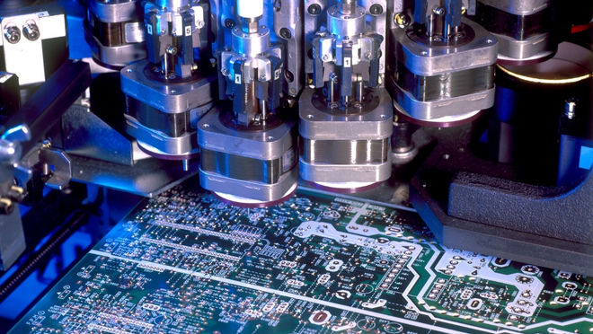
What Is PCB Layer Stack-Up?
The term “stack-up” in electronics refers to the vertical configuration of copper and dielectric (insulating) layers in a PCB. Each layer serves a specific function, such as signal routing, power distribution, or shielding. The arrangement and number of these layers determine the board’s electrical performance, mechanical strength, and ability to support complex circuits.
Typical stack-ups range from simple single- or double-sided boards to advanced multi-layer configurations with four, six, eight, or more layers. As devices become smaller and more complex, the need for carefully engineered stack-ups grows. The right stack-up can reduce electromagnetic interference (EMI), minimize signal loss, and enable higher-speed operation.
Key Principles of Electronics Stack-Up Design
Designing an effective stack-up involves balancing several competing requirements. Here are some of the most important considerations:
- Signal Integrity: Proper layer arrangement helps maintain clean, undistorted signals, especially in high-speed or high-frequency applications.
- Electromagnetic Compatibility (EMC): Strategic placement of ground and power planes can shield sensitive signals and reduce EMI.
- Thermal Management: Layer stack-up affects heat dissipation, which is critical for high-power or densely packed boards.
- Manufacturability: The chosen stack-up must be compatible with fabrication capabilities and cost constraints.
- Mechanical Strength: The number and type of layers contribute to the board’s rigidity and durability.

Common Layer Configurations in PCB Stack-Ups
There are several standard stack-up arrangements, each suited to different application needs. Here are a few typical examples:
2-Layer Boards
These are the simplest and most cost-effective, with one layer for components and traces on each side. They are suitable for basic circuits with low complexity and minimal EMI concerns.
4-Layer Stack-Ups
A common choice for more advanced designs, a 4-layer board usually consists of two outer signal layers and two inner planes (typically power and ground). This arrangement improves signal quality and EMI shielding, making it ideal for moderate-speed digital circuits.
6-Layer and Beyond
As circuit complexity increases, additional layers are added for extra signal routing and dedicated power or ground planes. High-speed, high-density, or RF boards often use 6, 8, or even more layers to achieve the necessary performance and reliability.

Benefits of Optimized Stack-Up Arrangements
Careful planning of the stack-up brings several advantages:
- Reduced Crosstalk: By placing ground planes adjacent to signal layers, unwanted coupling between traces is minimized.
- Improved Power Distribution: Dedicated power and ground layers ensure stable voltage and reduce noise.
- Enhanced EMI Control: Layer symmetry and shielding techniques help meet regulatory requirements for emissions and immunity.
- Better Signal Performance: Controlled impedance and reduced signal loss are possible with the right layer arrangement.
- Increased Design Flexibility: More layers allow for complex routing and integration of advanced features.
Design Process for Effective Stack-Ups
Creating a robust stack-up involves several steps:
- Define System Requirements: Consider speed, power, mechanical, and regulatory needs.
- Select Layer Count: Choose the minimum number of layers that meets electrical and mechanical goals.
- Assign Layer Functions: Decide which layers will carry signals, power, or ground.
- Determine Material Types: Select appropriate dielectrics and copper thickness based on performance and cost.
- Simulate and Validate: Use simulation tools to check impedance, EMI, and thermal performance.
- Review Manufacturability: Ensure the stack-up can be fabricated reliably and within budget.
For those new to PCB fundamentals, the PCB basics tutorial from SparkFun offers a helpful introduction to the core concepts and terminology.
Challenges and Best Practices in Layer Stack Planning
While the benefits of a well-designed stack-up are clear, several challenges can arise:
- Cost vs. Performance: More layers and advanced materials increase cost, so balance is essential.
- Fabrication Limits: Not all manufacturers can produce boards with very thin dielectrics or many layers.
- Signal Integrity Issues: Poorly planned stack-ups can lead to reflections, ringing, or excessive EMI.
- Thermal Concerns: Dense boards may require special materials or heat-spreading techniques.
To address these, follow these best practices:
- Work closely with your PCB fabricator to understand their capabilities and constraints.
- Use simulation tools early in the design process to predict and solve signal or thermal issues.
- Document your stack-up choices clearly for manufacturing and testing teams. For guidance on documentation, refer to our electronic product design documentation workflow.
- Consider future revisions and scalability when selecting materials and layer counts.
Integrating Stack-Up Design with Product Development
Layer arrangement is not an isolated task; it should be coordinated with the overall product development cycle. Early stack-up decisions affect enclosure design, thermal management, and compliance testing. Collaboration between electrical, mechanical, and manufacturing teams ensures that the final product meets all requirements without costly redesigns.
Testing is a critical part of this process. For more on how stack-up choices impact verification, see our electronic product design performance testing guide and electronic product design environmental testing guide.
Frequently Asked Questions
What is the main purpose of a PCB stack-up?
The primary goal of a stack-up is to optimize the electrical, mechanical, and thermal properties of a circuit board. By carefully arranging layers, designers can control impedance, minimize EMI, and ensure reliable operation in demanding environments.
How does stack-up affect signal integrity?
Layer arrangement determines how signals travel through the board. Placing ground planes close to signal layers reduces noise and crosstalk, while controlled dielectric thickness helps maintain consistent impedance for high-speed signals.
Can stack-up design reduce manufacturing costs?
Yes, choosing the right number of layers and materials can lower production costs by simplifying fabrication and assembly. However, cutting corners on stack-up can lead to performance issues, so it’s important to balance cost with technical requirements.
Conclusion
Effective electronics stack-up design is a cornerstone of reliable, high-performance electronic products. By understanding the principles, common configurations, and best practices, engineers can create PCBs that meet demanding technical and commercial goals. Integrating stack-up planning with system-level design, documentation, and testing ensures that products are robust, manufacturable, and ready for market success.