

The process of assembling electronic products is a complex, multi-stage journey that transforms raw components into reliable, functional devices. Understanding the electronics assembly workflow is essential for engineers, product managers, and anyone involved in electronics manufacturing. This guide breaks down each phase, highlights best practices, and explores how careful planning and execution can lead to higher quality and efficiency.
Whether you’re new to the field or seeking to optimize your current processes, a clear grasp of the steps involved—from design validation to final inspection—can help you avoid costly mistakes and improve product outcomes. For those interested in the broader context of product development, the electronic product design performance testing guide provides valuable insights into ensuring that assembled devices meet rigorous standards.

Key Stages in the Electronics Assembly Process
The journey from concept to finished electronic product involves several crucial steps. Each stage in the electronics assembly workflow builds on the previous one, ensuring that the final product is both functional and reliable. Here’s a closer look at the main phases:
1. Design Review and Bill of Materials Preparation
Every successful assembly project starts with a thorough review of the product’s design files and documentation. This includes checking schematics, layout files, and the bill of materials (BOM). The BOM lists all required parts, their specifications, and approved vendors. Any discrepancies or ambiguities at this stage can cause delays or errors later on.
- Verify schematic and PCB layout accuracy
- Ensure component availability and compatibility
- Confirm manufacturing tolerances and assembly constraints
2. Sourcing and Incoming Quality Control
Once the BOM is finalized, components are sourced from trusted suppliers. Upon arrival, incoming parts undergo quality checks to detect any defects or counterfeit items. This step is critical for maintaining the integrity of the assembly process.
- Visual inspection for damage or labeling errors
- Electrical testing of sensitive components
- Documentation and traceability for each batch
3. PCB Fabrication and Preparation
Printed circuit boards (PCBs) form the backbone of most electronic products. PCB fabrication involves etching copper traces, drilling holes, and applying solder masks according to the design files. After fabrication, boards are cleaned and prepared for component placement.
For more information on selecting the right PCB materials, see the electronic product design pcb material selection guide.
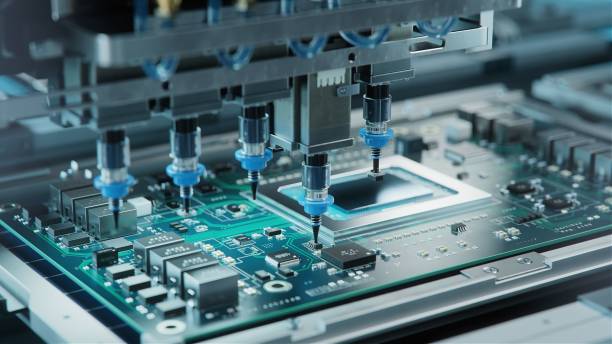
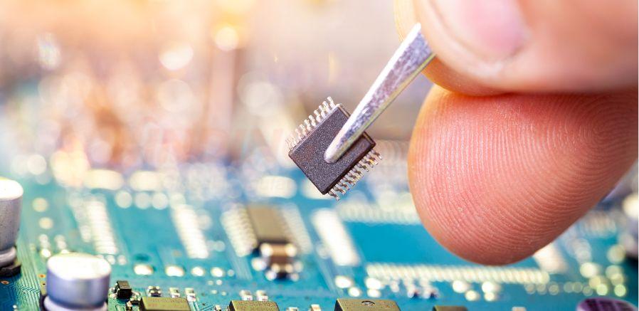
Component Placement and Soldering Techniques
With PCBs ready and components inspected, the next step is to mount parts onto the board. This phase of the electronics assembly workflow can be performed manually or with automated equipment, depending on the complexity and volume of production.
Surface Mount Technology (SMT)
SMT is the most common method for placing components on modern PCBs. Automated pick-and-place machines position tiny parts onto solder paste deposits, after which the assembly passes through a reflow oven to melt the solder and secure the components.
- High speed and accuracy for large production runs
- Minimizes human error and increases consistency
- Supports miniaturization and dense layouts
Through-Hole Assembly
Some components, such as connectors or large capacitors, require through-hole mounting. Leads are inserted into pre-drilled holes and soldered, often using wave soldering machines for efficiency. This method provides strong mechanical bonds, making it ideal for parts subject to physical stress.
Mixed Technology and Specialized Processes
Many products use both SMT and through-hole components. In these cases, assembly lines are configured to handle both processes efficiently. Additional steps, such as selective soldering or manual rework, may be required for complex or sensitive parts.
Inspection, Testing, and Quality Assurance
Quality control is embedded throughout the electronics assembly workflow. After soldering, assemblies undergo various inspections and tests to ensure functionality and reliability.
- Automated Optical Inspection (AOI): Cameras scan the board for misplaced components, solder defects, or missing parts.
- In-Circuit Testing (ICT): Electrical probes verify that each component is correctly installed and functioning.
- Functional Testing: Simulates real-world operating conditions to confirm that the device performs as intended.
- X-ray Inspection: Used for hidden solder joints, such as those under BGAs (Ball Grid Arrays).
For a deeper dive into performance validation, refer to the electronic product design performance testing guide.
Final Assembly, Packaging, and Logistics
Once PCB assemblies pass all inspections, they are integrated into their enclosures, connected with other modules, and subjected to a final round of quality checks. This stage may also include firmware loading, labeling, and packaging for shipment.
- Mechanical integration and enclosure assembly
- Final visual and functional inspections
- ESD-safe packaging and labeling
- Logistics coordination for delivery to customers or distribution centers
If you’re interested in how mechanical considerations impact this phase, the electronic product mechanical integration guide offers practical advice.
Best Practices for Streamlining the Assembly Workflow
Improving efficiency and product quality requires attention to detail at every stage. Here are some proven strategies for optimizing the electronics assembly workflow:
- Maintain clear and up-to-date documentation for all product revisions
- Foster close collaboration between design, procurement, and manufacturing teams
- Invest in automated inspection and testing equipment
- Implement traceability systems for components and assemblies
- Regularly review and refine processes based on feedback and data
For additional technical resources on electronics manufacturing, explore this comprehensive electronics tutorials site.
Frequently Asked Questions
What is the difference between SMT and through-hole assembly?
Surface Mount Technology (SMT) uses automated machines to place components directly onto the surface of a PCB, making it ideal for high-volume and miniaturized products. Through-hole assembly involves inserting component leads into holes and soldering them, which provides stronger mechanical support and is often used for connectors or large parts.
How can manufacturers ensure quality in electronics assembly?
Quality is maintained through a combination of incoming material inspection, automated and manual testing, and thorough documentation. Automated Optical Inspection (AOI), In-Circuit Testing (ICT), and functional tests are standard practices. Traceability and process control also play key roles in preventing defects.
Why is documentation important in the assembly workflow?
Accurate and up-to-date documentation ensures that all teams are working from the same information, reduces errors, and speeds up troubleshooting. It also supports regulatory compliance and makes it easier to implement design changes or address issues during production.
Conclusion
Mastering the electronics assembly workflow is essential for delivering high-quality, reliable products to market. By understanding each phase—from design review and sourcing to testing and final packaging—manufacturers can minimize errors, reduce costs, and meet customer expectations. Staying informed about best practices and leveraging the right resources will help you keep pace with evolving technology and industry standards.