

Designing a reliable and efficient printed circuit board (PCB) is a critical step in the development of any modern electronic device. The layout process directly impacts product performance, manufacturability, and long-term reliability. By following electronic product PCB layout best practices, engineers can minimize costly errors, reduce electromagnetic interference, and ensure seamless integration with other system components.
Whether you are developing a consumer gadget, industrial controller, or IoT device, understanding the principles of effective PCB design is essential. This article provides a comprehensive overview of proven techniques, from schematic capture to final layout checks, to help you create robust and production-ready circuit boards.
For a deeper dive into integrating your PCB with the rest of your device, see our electronic product design system integration guide, which covers system-level considerations and practical integration tips.
Key Principles for Reliable PCB Design
Adhering to fundamental guidelines is the foundation of any successful PCB project. Here are some of the most important considerations to keep in mind:
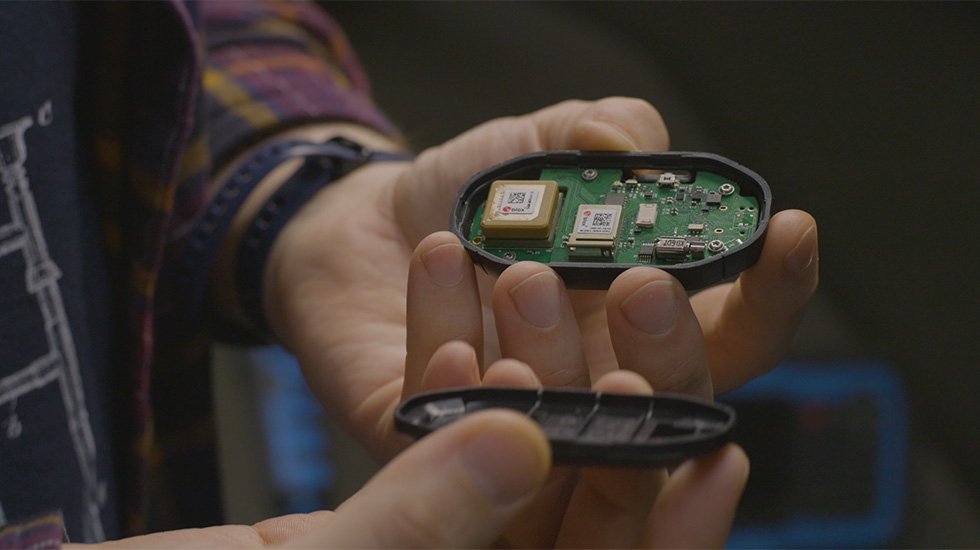
- Component Placement: Arrange parts logically, grouping related components and minimizing signal path lengths. Place sensitive analog circuits away from noisy digital sections.
- Signal Integrity: Route high-speed signals with controlled impedance and avoid sharp corners or stubs. Use ground planes to reduce noise and crosstalk.
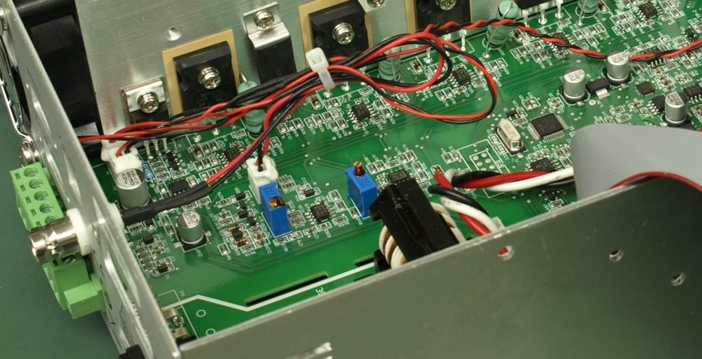
- Power Distribution: Implement solid power and ground planes, and decouple ICs with capacitors placed close to their supply pins.
- Thermal Management: Position heat-generating components to optimize airflow and use thermal vias or copper pours to dissipate heat.
- Design for Manufacturability (DFM): Follow standard footprints, maintain adequate spacing, and avoid unnecessarily complex shapes or features.
Optimizing Component Placement and Routing
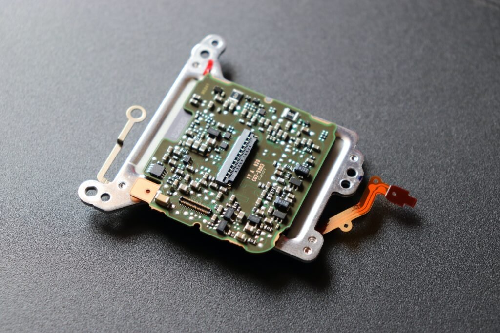
Effective component placement is a cornerstone of PCB layout best practices for electronic products. Start by placing connectors, switches, and other interface elements according to the product’s mechanical requirements. Next, position critical components such as microcontrollers, power regulators, and oscillators, ensuring short and direct signal paths.
When routing traces, prioritize the following:
- Keep high-frequency and sensitive analog signals short and direct.
- Route differential pairs together, maintaining consistent spacing and length.
- Use wider traces for power lines to reduce voltage drop and heating.
- Minimize the number of vias, as each via adds resistance and inductance.
For more on documentation and workflow, refer to our electronic product design documentation workflow guide.
Power Integrity and Grounding Strategies
Maintaining clean and stable power delivery is essential for any electronic device. Use dedicated power and ground planes whenever possible, as they provide low-impedance paths and help shield sensitive signals. Decoupling capacitors should be placed as close as possible to each IC’s power pins to suppress voltage spikes and noise.
When laying out ground returns, avoid creating ground loops, which can introduce unwanted interference. Star grounding, where all ground connections converge at a single point, is effective for many designs. For multilayer boards, ensure that ground planes are continuous and not fragmented by signal traces.
Managing Electromagnetic Interference (EMI)
Electromagnetic compatibility is a major concern in modern electronics. To reduce EMI, follow these strategies:
- Keep high-speed signals away from analog and low-frequency lines.
- Use ground fills and guard traces to shield sensitive areas.
- Route clock and data lines over continuous ground planes.
- Minimize loop areas by routing return paths directly under signal traces.
Shielding critical sections and using proper filtering components can further reduce emissions and susceptibility to external noise. For a comparison of safety standards, see our electronic product design safety standards comparison.
Thermal Considerations in PCB Layout
As power densities increase, thermal management becomes increasingly important. Place heat-generating parts, such as voltage regulators and power transistors, in areas with good airflow. Use large copper pours, thermal vias, and heat sinks where necessary to draw heat away from sensitive components.
Simulate thermal performance early in the design process to identify potential hotspots. Proper thermal design not only improves reliability but also extends the operational life of your product.
Design for Testability and Manufacturability
Ensuring your PCB can be easily tested and manufactured is just as important as its electrical performance. Here are some tips:
- Include test points for critical signals and power rails.
- Maintain clear silkscreen markings for component identification.
- Follow recommended spacing and clearance rules to prevent solder bridging and shorts.
- Use standard component footprints and avoid custom shapes unless necessary.
Early collaboration with your manufacturing partner can help identify potential issues and streamline the production process. For more on reliability, see our electronic product design reliability engineering basics.
Verification, Testing, and Documentation
Before sending your design to fabrication, run thorough design rule checks (DRC) and electrical rule checks (ERC) in your PCB design software. Simulate signal integrity and power distribution to catch issues early. After assembly, functional testing and in-circuit testing help ensure the board operates as intended.
Comprehensive documentation, including schematics, layout files, and assembly instructions, is vital for troubleshooting, future revisions, and regulatory compliance. For a step-by-step guide, see our electronic product design performance testing guide.
Staying Updated with Industry Trends
The field of PCB design is constantly evolving, with new materials, manufacturing techniques, and design tools emerging regularly. Staying informed about the latest advancements can help you adopt more efficient processes and improve your product’s competitiveness. For a broader perspective on electronic product development, consider reading this comprehensive guide to electronic product design.
Frequently Asked Questions
What are the most common mistakes in PCB layout for electronic products?
Some frequent errors include poor component placement, inadequate power and ground distribution, insufficient trace width for high-current paths, and neglecting signal integrity for high-speed lines. Overlooking thermal management and failing to follow design for manufacturability guidelines can also lead to costly revisions.
How can I reduce electromagnetic interference in my PCB design?
To minimize EMI, keep high-speed signals short and well-shielded, use continuous ground planes, and separate analog and digital sections. Implementing proper filtering and shielding, as well as careful routing of return paths, further helps reduce emissions and susceptibility to noise.
Why is documentation important in PCB layout?
Accurate documentation ensures that the design intent is clearly communicated to manufacturers, assemblers, and future engineers. It helps prevent errors during production, simplifies troubleshooting, and supports compliance with industry standards and certifications.