

Designing modern electronics requires careful attention to electromagnetic interference (EMI). As devices become more compact and feature-rich, the risk of unwanted electromagnetic emissions and susceptibility to external noise increases. This comprehensive guide explores the essential principles, best practices, and practical steps for minimizing EMI in electronic product development. Whether you are an engineer, product manager, or quality specialist, understanding EMI is crucial for ensuring product reliability, regulatory compliance, and customer satisfaction.
For those interested in a broader perspective on the development process, the electronic product design performance testing guide offers valuable insights into testing strategies that complement EMI mitigation.
Understanding Electromagnetic Interference in Device Development
Electromagnetic interference refers to the unwanted disturbance that affects an electrical circuit due to electromagnetic radiation emitted from an external source. In the context of electronic product design, EMI can degrade performance, cause malfunctions, or even lead to regulatory non-compliance. Sources of EMI include switching power supplies, high-speed digital circuits, wireless transmitters, and even nearby electronic devices.
EMI can be categorized as either conducted (transmitted through physical connections like wires or PCB traces) or radiated (emitted through the air). Both types can disrupt sensitive circuits, leading to data errors, loss of functionality, or safety hazards.
Key Principles for Minimizing EMI in Electronic Product Design
Effective EMI control starts at the design phase. By following proven engineering principles, teams can reduce the risk of interference and streamline the path to compliance. Here are the foundational concepts:
- Grounding and Shielding: Establish a low-impedance ground path and use shields to block or redirect electromagnetic fields.
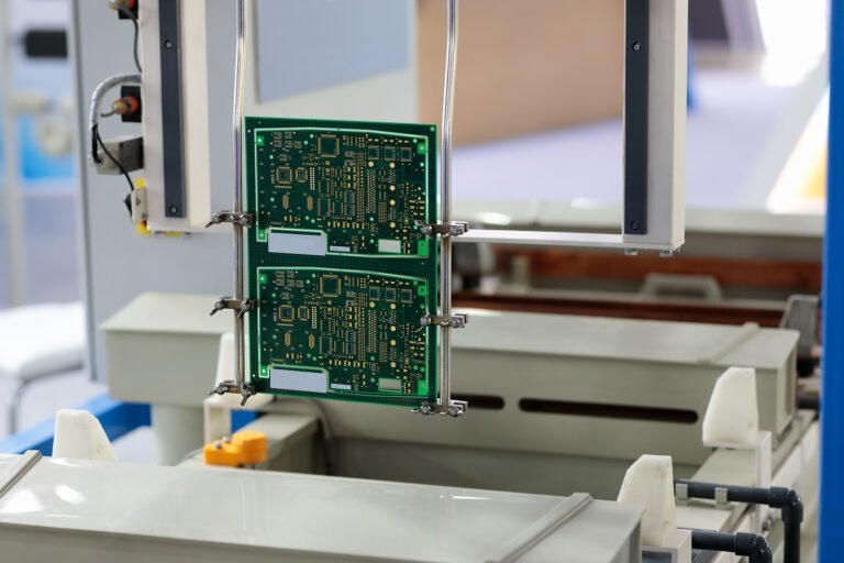
- PCB Layout Optimization: Keep high-speed signal traces short, use ground planes, and separate analog and digital sections.
- Filtering: Apply capacitors, ferrite beads, and other filters to suppress unwanted frequencies.
- Cable Management: Route cables away from noise sources and use twisted pairs or shielded cables where appropriate.
- Component Placement: Position sensitive components away from high-frequency or high-current areas.
For a deeper dive into material choices that impact EMI, the electronic product design pcb material selection resource provides detailed guidance on substrate selection and its effect on electromagnetic performance.
Design Strategies for Electromagnetic Compatibility
Achieving electromagnetic compatibility (EMC) is a central goal in any electronic product design electromagnetic interference guide. EMC ensures that a device functions properly in its intended environment without causing or suffering from EMI. Consider these strategies:
1. Layered PCB Design
Using multi-layer PCBs with dedicated ground and power planes helps contain electromagnetic fields and provides effective return paths for high-frequency signals. This reduces loop areas, which are a common source of radiated emissions.
2. Controlled Impedance and Signal Integrity
Designing traces with controlled impedance minimizes signal reflections and crosstalk, both of which can contribute to EMI. Differential signaling and proper termination further enhance noise immunity.
3. Enclosure Shielding
Metal or conductive enclosures act as Faraday cages, blocking external EMI and containing internal emissions. Ensure that seams and openings are minimized or properly gasketed to maintain shielding effectiveness.
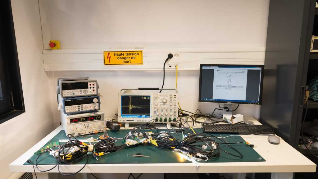
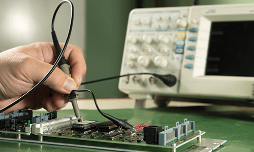
Testing and Compliance for EMI in Product Development
EMI testing is a critical step before launching any electronic product. Regulatory bodies such as the FCC (USA), CE (Europe), and others require products to meet strict emission and immunity standards. Testing typically includes:
- Pre-compliance Testing: Early-stage tests to identify and resolve EMI issues before formal certification.
- Conducted Emissions: Measuring unwanted signals on power and signal lines.
- Radiated Emissions: Assessing electromagnetic energy emitted through the air.
- Immunity Testing: Ensuring the device can withstand external electromagnetic disturbances.
Integrating EMI testing into the development cycle reduces costly redesigns and accelerates time-to-market. For more on the broader development process, the comprehensive overview of electronic product design and development provides additional context and best practices.
Common EMI Challenges and Solutions
Even with careful planning, EMI issues can arise. Here are some frequent challenges and practical solutions:
| Challenge | Solution |
|---|---|
| High-Frequency Noise on Power Lines | Use decoupling capacitors close to IC power pins and apply ferrite beads on power traces. |
| Unintentional Antenna Effects | Minimize loop areas, avoid long parallel traces, and use ground fills. |
| Susceptibility to External EMI | Implement shielding, use robust filtering, and select components with high immunity ratings. |
| PCB Crosstalk | Increase spacing between high-speed traces and use ground planes to isolate signals. |
Integrating EMI Considerations with the Product Lifecycle
Addressing EMI is not a one-time task but an ongoing process throughout the product lifecycle. Early design reviews, iterative prototyping, and collaboration between hardware, firmware, and mechanical teams are essential. Consider referencing the electronic product lifecycle cost analysis guide to understand how EMI mitigation impacts long-term costs and product sustainability.
Best Practices for EMI Management in Electronics
- Start EMI planning at the concept stage, not after the first prototype.
- Document all design decisions related to EMI for future reference and troubleshooting.
- Use simulation tools to predict EMI behavior before physical testing.
- Train all team members on basic EMI principles to foster a culture of electromagnetic compatibility.
- Stay updated on evolving standards and regulatory requirements in your target markets.
Frequently Asked Questions
What is the difference between EMI and EMC?
EMI (electromagnetic interference) is the unwanted disturbance caused by electromagnetic emissions, while EMC (electromagnetic compatibility) is the ability of a device to function properly in its environment without causing or being affected by EMI. Achieving EMC means managing EMI effectively.
Why is EMI testing important in electronic product development?
EMI testing ensures that products meet regulatory standards, function reliably, and do not interfere with other devices. Early and thorough testing helps avoid costly redesigns and market delays.
How can PCB layout help reduce EMI?
Optimizing PCB layout by minimizing trace lengths, using ground planes, separating analog and digital sections, and careful component placement can significantly reduce both conducted and radiated EMI.
Conclusion
Minimizing electromagnetic interference is a foundational aspect of successful electronic product design. By applying robust design principles, integrating EMI considerations throughout the development cycle, and staying informed about compliance requirements, teams can deliver reliable, high-performance products. For additional insights into localization and integration, explore the electronic product localization considerations and electronic product mechanical integration guide resources.