

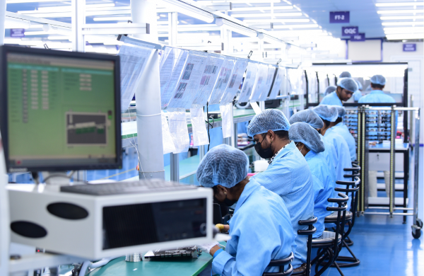
In the electronics manufacturing industry, efficiency and precision are essential for delivering high-quality products at scale. One critical process that supports these goals is PCB panelization. This technique involves grouping multiple printed circuit boards (PCBs) onto a single larger substrate, allowing them to be fabricated, assembled, and tested together. By understanding how panelization works, manufacturers and designers can optimize production, reduce costs, and minimize waste.
For those interested in broader design and testing strategies, the electronic product design performance testing guide offers further insights into ensuring reliable and robust electronic assemblies.
Understanding the Concept of PCB Panelization
At its core, PCB panelization is the practice of arranging several smaller circuit boards onto a single, larger panel. This approach streamlines the manufacturing process by enabling multiple boards to be processed simultaneously through fabrication, assembly, and testing steps. Once all operations are complete, the individual boards are separated, or “depanelized,” for final use.
The main reasons for using this method include:
- Increased throughput: Multiple boards are handled as a unit, speeding up production.
- Reduced handling: Fewer manual interventions lower the risk of damage and defects.
- Cost savings: Shared panel space and batch processing can lower overall manufacturing expenses.
- Consistency: Uniform processing leads to higher quality and repeatability.
Why Panelization Matters in Electronics Manufacturing
The benefits of grouping multiple boards on a single panel extend beyond just efficiency. For manufacturers, panelization is a strategic choice that impacts several aspects of the production cycle:
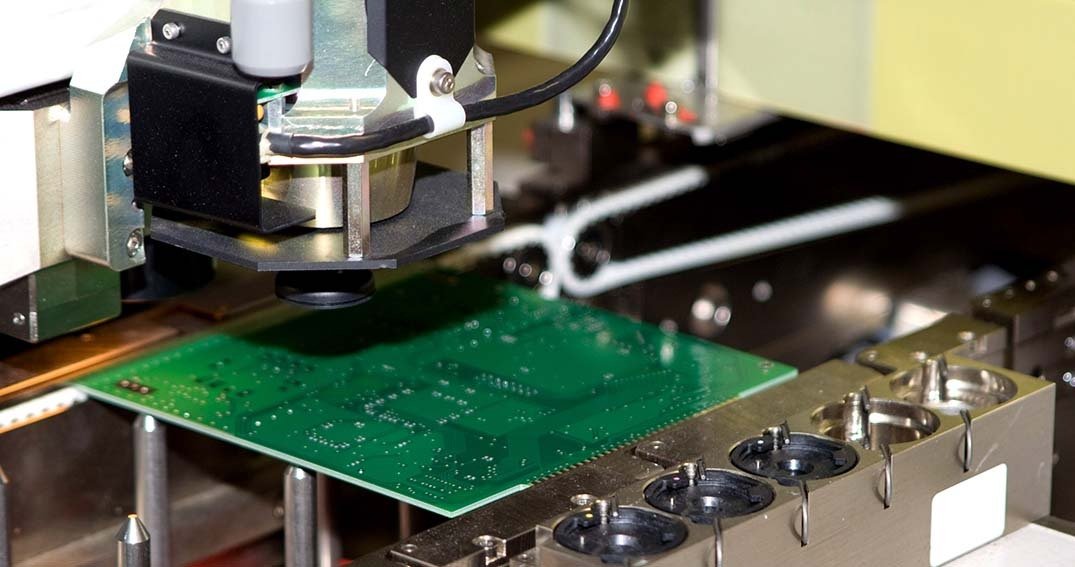
- Optimized machine utilization: Automated assembly equipment, such as pick-and-place machines, can process entire panels at once, maximizing throughput.
- Streamlined testing: Functional and in-circuit tests can be performed on all boards in a panel, reducing setup time and labor.
- Minimized material waste: By carefully arranging boards and minimizing gaps, manufacturers use raw materials more efficiently.
- Improved handling: Larger panels are easier to transport and less prone to damage compared to handling many small boards individually.
For companies managing the entire product lifecycle, integrating panelization with other strategies—such as those discussed in the electronic product lifecycle cost analysis guide—can further enhance cost control and product quality.
Common Panelization Techniques and Methods
There are several ways to arrange and separate PCBs within a panel, each with its own advantages and considerations. The choice depends on the board design, assembly requirements, and the intended depanelization method.
V-Scoring
V-scoring involves cutting shallow grooves along the lines where boards will be separated. After assembly, the boards are snapped apart. This method is fast and cost-effective, but it is best suited for rectangular boards and may not be ideal for complex shapes.
Tab-Routing
In tab-routing, small tabs connect each board to the panel frame. These tabs can include perforations (mouse bites) to make breaking them easier. Tab-routing accommodates irregular board shapes and reduces stress during separation, but it may require additional finishing to smooth the edges.
Combination Approaches
Sometimes, manufacturers use a mix of V-scoring and tab-routing to balance ease of separation with panel strength. The choice depends on the product’s requirements and the capabilities of the manufacturing facility.
Design Considerations for Effective PCB Panelization
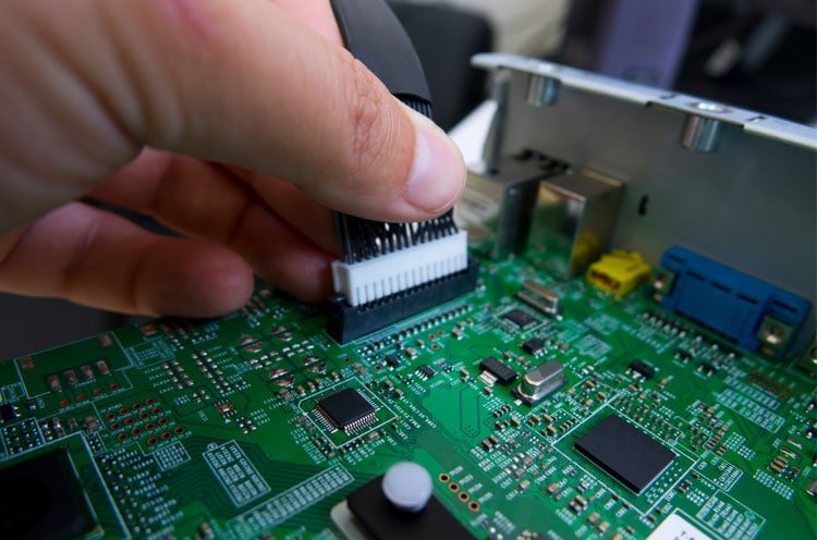
Successful panelization starts at the design stage. Engineers and designers must consider several factors:
- Board outline and shape: Irregular shapes may require tab-routing or custom panel layouts.
- Component placement: Components should not be placed too close to panel edges or separation lines to avoid damage during depanelization.
- Panel size: The overall panel must fit within the capabilities of the fabrication and assembly equipment.
- Fiducials and tooling holes: These features ensure accurate alignment and handling throughout the process.
- Depanelization method: The chosen method (V-scoring, tab-routing, or both) affects how the boards are separated and finished.
For more on material choices and their impact on manufacturing, see the electronic product design pcb material selection guide.
Challenges and Best Practices in Panelization
While panelization offers many advantages, it also introduces certain challenges. Warping, uneven stress during depanelization, and improper spacing can lead to defects or damaged boards. To mitigate these risks, manufacturers should:
- Collaborate closely with PCB fabricators to ensure panel layouts are compatible with their processes.
- Use adequate spacing between boards and avoid placing sensitive components near separation lines.
- Select the most suitable depanelization method based on board geometry and assembly needs.
- Test panel designs with prototypes before committing to full-scale production.
For those new to electronics assembly, resources like this beginner’s guide to electronics projects can provide additional context on manual and automated assembly techniques.
Applications and Impact of PCB Panelization in Industry
The use of panelization is widespread in industries ranging from consumer electronics to automotive and medical devices. By enabling high-volume, repeatable manufacturing, this process supports the rapid development and deployment of modern electronic products. It also plays a key role in cost management, quality assurance, and supply chain efficiency.
As products become more complex and miniaturized, the importance of careful panelization design continues to grow. Integrating this process with other manufacturing best practices—such as those covered in the electronic product mechanical integration guide—can help companies stay competitive in a fast-evolving market.
Frequently Asked Questions
How does PCB panelization improve manufacturing efficiency?
By grouping multiple boards on a single panel, manufacturers can process, assemble, and test several units at once. This reduces handling time, increases throughput, and lowers the risk of errors, leading to more efficient production.
What are the main methods for separating boards after panelization?
The two most common methods are V-scoring and tab-routing. V-scoring uses shallow grooves for easy snapping, while tab-routing connects boards with small tabs that are broken or cut after assembly. The choice depends on board shape and assembly requirements.
What design factors should be considered for successful panelization?
Key considerations include board outline, component placement, panel size, spacing, and the intended depanelization method. Proper planning ensures that boards can be manufactured and separated without damage or defects.
