

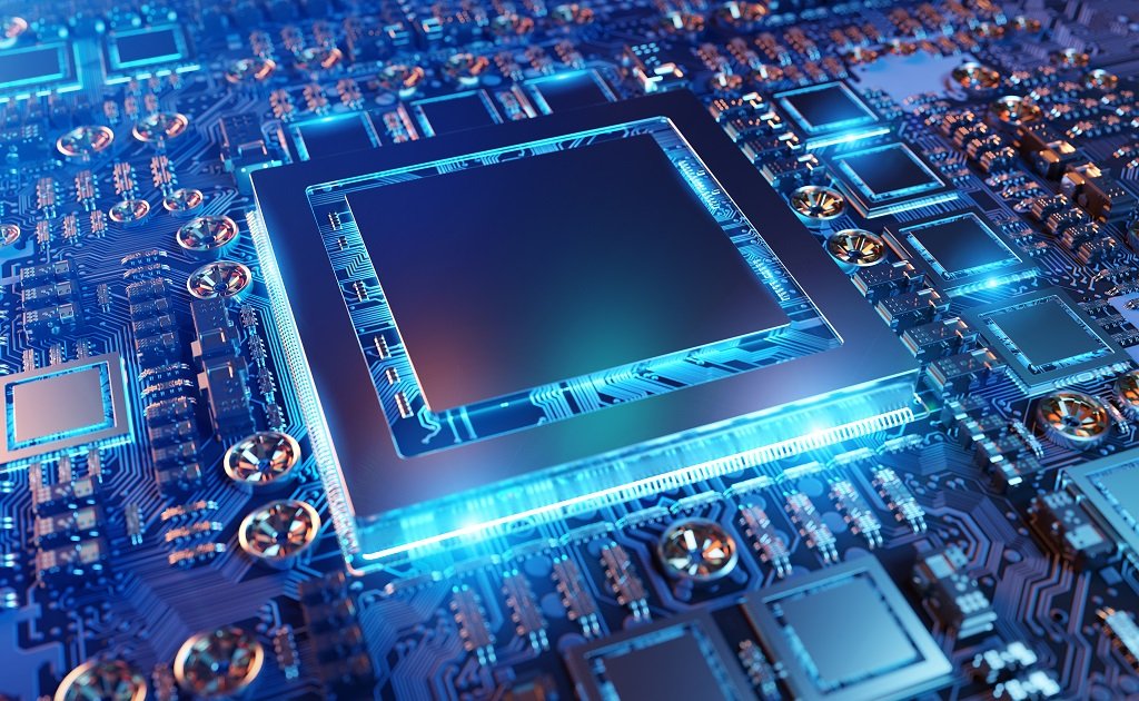
High-Density Interconnect (HDI) printed circuit boards (PCBs) have become a cornerstone in modern electronics, offering a multitude of advantages that cater to the demands of today’s compact and high-performance devices. As technology continues to evolve, the need for smaller, more efficient, and reliable electronic components has driven the adoption of HDI PCBs across various industries.
In this guide, we will explore the reasons behind the growing popularity of HDI PCBs, their benefits, and how they contribute to advancements in electronic design and manufacturing. For those interested in understanding the broader context of electronic product design, our electronic product design performance testing guide provides additional insights.
Understanding the Benefits of HDI PCBs
HDI PCBs are renowned for their ability to support higher wiring density, which is crucial for the miniaturization of electronic products. This increased density allows for more components to be placed on a smaller board, which is essential for modern devices like smartphones, tablets, and wearable technology.
One of the primary benefits of HDI technology is its ability to enhance electrical performance. By reducing the distance between components, HDI PCBs minimize signal loss and improve signal integrity. This is particularly important in high-speed applications where data transmission accuracy is critical.
Applications in Various Industries
The versatility of HDI PCBs makes them suitable for a wide range of applications. In the consumer electronics sector, they are used in devices that require compact designs without compromising functionality. In the automotive industry, HDI PCBs are integral to the development of advanced driver-assistance systems (ADAS) and infotainment systems.
Moreover, the medical field benefits from HDI technology in the creation of compact medical devices that require precise and reliable performance. These applications highlight the critical role that HDI PCBs play in advancing technology across different sectors.
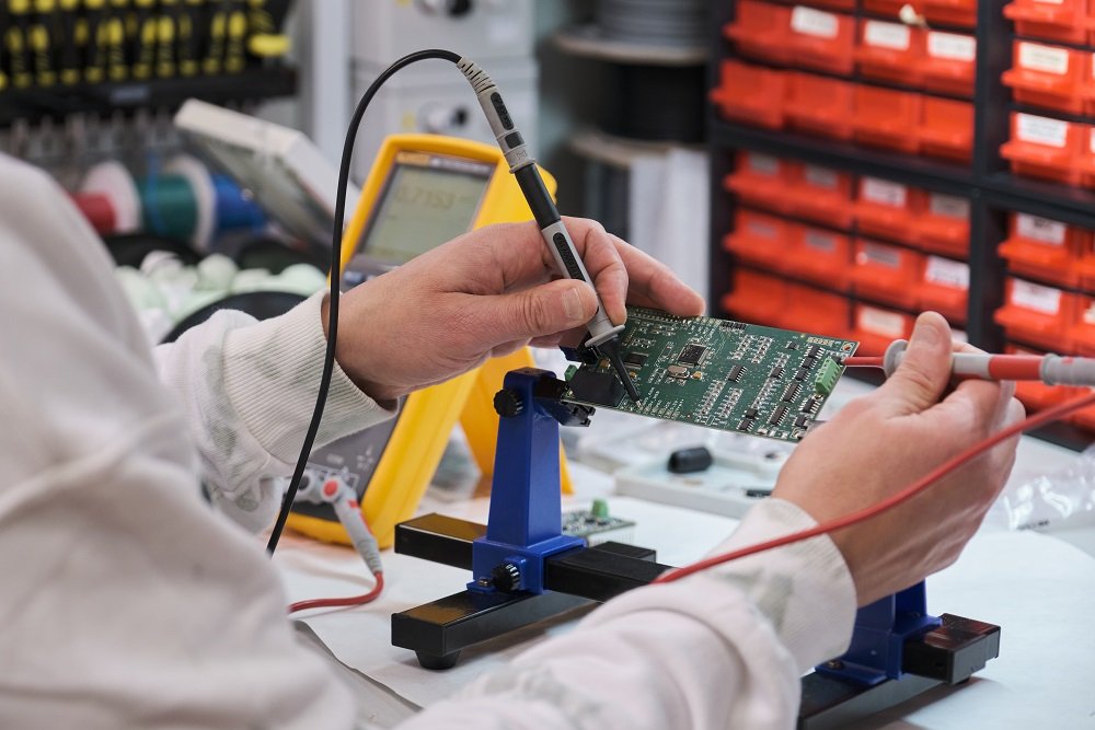
Design and Manufacturing Considerations
Designing HDI PCBs involves several considerations to ensure optimal performance. The choice of materials, layer stack-up, and via technology are critical factors that influence the board’s capabilities. For more detailed information on selecting the right materials, our electronic product design PCB material selection guide offers comprehensive guidance.
Manufacturers must also consider the precision required in the fabrication process. The use of microvias, blind and buried vias, and laser drilling techniques are common in HDI PCB production, allowing for the creation of intricate designs that meet the demands of modern electronics.
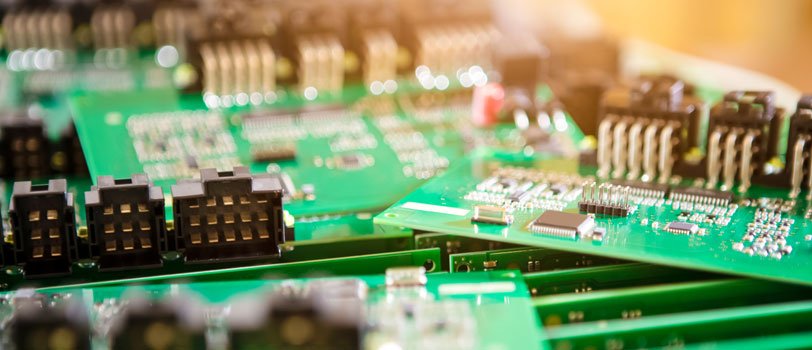
Future Trends in HDI PCB Technology
As the demand for more sophisticated electronic devices grows, HDI PCB technology is expected to continue evolving. Emerging trends include the integration of flexible and rigid-flex designs, which offer additional versatility in product design. Furthermore, advancements in semiconductor fabrication processes, as detailed in this comprehensive guide, are likely to influence the future development of HDI PCBs.
These innovations will enable manufacturers to produce even more compact and efficient electronic products, meeting the ever-increasing expectations of consumers and industries alike.
FAQs
What are the main advantages of using HDI PCBs?
HDI PCBs offer several advantages, including higher wiring density, improved electrical performance, and the ability to support miniaturization of electronic devices. These benefits make them ideal for applications in consumer electronics, automotive, and medical industries.
How do HDI PCBs improve signal integrity?
By reducing the distance between components, HDI PCBs minimize signal loss and enhance signal integrity. This is crucial for high-speed applications where accurate data transmission is essential.
What future trends are expected in HDI PCB technology?
Future trends in HDI PCB technology include the integration of flexible and rigid-flex designs, as well as advancements in semiconductor fabrication processes. These developments will enable the production of more compact and efficient electronic products.
