

PCB design in electronic product development plays a pivotal role in transforming innovative concepts into functional, manufacturable devices. As electronics become more compact and complex, the quality and efficiency of printed circuit board layouts directly impact product performance, reliability, and cost. Whether developing consumer gadgets, industrial controls, or IoT solutions, understanding the essentials of PCB layout and integration is critical for successful product launches.
This article explores the core stages, considerations, and best practices for integrating PCB design into the broader electronic development process. Early attention to layout, component selection, and manufacturability helps prevent costly revisions and accelerates time to market. For those seeking a broader context on how system integration fits into the process, the electronic product design system integration guide provides additional insights.
Understanding the Role of PCB Design in Product Development
The printed circuit board is the backbone of any electronic device, providing both the physical platform and the electrical interconnections for components. During development, the PCB layout must balance electrical performance, mechanical constraints, and manufacturing requirements. Early collaboration between design, engineering, and manufacturing teams ensures that the board supports all functional and regulatory needs.
Key responsibilities of PCB layout in product creation include:
- Defining the placement and routing of components to optimize signal integrity and minimize noise
- Ensuring mechanical fit within the product enclosure
- Supporting thermal management and power distribution
- Facilitating efficient assembly and testing
For a more detailed look at the broader process, consider reviewing this comprehensive overview of electronic product design.
Key Stages of PCB Layout in Electronic Projects
Integrating pcb design in electronic product development involves several distinct phases. Each stage requires careful planning and validation to avoid downstream issues and ensure a smooth transition from concept to production.
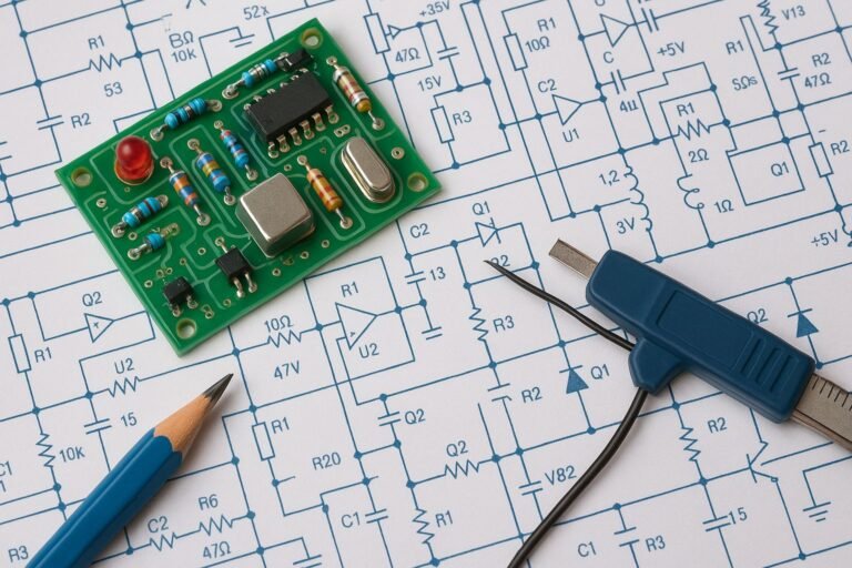
1. Schematic Capture and Component Selection
The process begins with schematic capture, where the electrical circuit is defined. Selecting appropriate components is crucial, as their footprints, electrical characteristics, and availability will influence the board layout and overall product cost. Designers must also consider regulatory and environmental requirements at this stage.
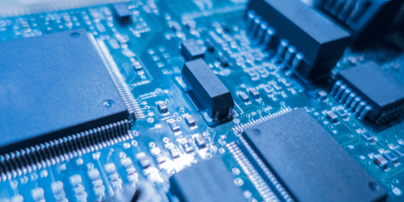
2. Board Layout and Routing
Once the schematic is complete, the physical arrangement of components on the board is determined. Proper placement is essential for signal integrity, thermal management, and manufacturability. Routing the electrical connections (traces) between components is a critical task, requiring attention to trace width, spacing, and layer stack-up to prevent interference and ensure reliable operation.
3. Design Rule Checks and Validation
Automated design rule checks (DRC) are used to verify that the layout meets electrical and manufacturing constraints. Signal integrity analysis, power distribution checks, and thermal simulations help identify potential issues before fabrication. Early validation reduces the risk of costly redesigns later in the process.
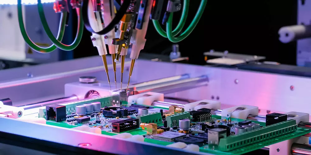
4. Prototyping and Testing
After layout approval, prototypes are manufactured for functional and performance testing. This phase allows engineers to validate the design under real-world conditions, identify any unforeseen issues, and refine the product as needed. For more on this critical step, the electronic product design performance testing guide offers practical advice.
Best Practices for Effective PCB Integration
To achieve reliable, cost-effective, and scalable products, it’s important to follow established best practices throughout the PCB development process. These strategies help minimize errors, streamline production, and ensure compliance with industry standards.
- Early Design for Manufacturability (DFM): Involve manufacturing partners early to ensure the board can be produced efficiently and at scale.
- Clear Documentation: Maintain up-to-date design files, assembly drawings, and bills of materials. For workflow tips, see the electronic product design documentation workflow.
- Iterative Prototyping: Test early and often to catch issues before mass production.
- Compliance and Testing: Design with regulatory standards in mind, including safety, EMC, and environmental requirements. The electronic product design safety standards comparison can help clarify requirements.
- Global Market Considerations: Adapt designs for international standards and supply chains. For more, see electronic product design for global markets.
Common Challenges in PCB Layout for Electronics
Even experienced teams encounter hurdles when integrating PCB layouts into new products. Some of the most frequent challenges include:
- Signal Integrity Issues: High-speed signals can suffer from crosstalk, reflections, or electromagnetic interference if not routed carefully.
- Thermal Management: Power-dense designs require careful attention to heat dissipation, especially in compact enclosures.
- Component Sourcing: Supply chain disruptions or obsolete parts can force last-minute changes, impacting layout and timelines.
- Mechanical Constraints: Fitting the board into a custom enclosure may require creative layout solutions or multiple design iterations.
Addressing these issues early and collaborating across disciplines helps ensure a smoother path from prototype to production.
Emerging Trends in PCB Development
The field of PCB layout is evolving rapidly, driven by advances in materials, manufacturing, and design automation. Some notable trends include:
- Miniaturization: Increasing demand for smaller, lighter products is pushing the limits of board density and component packaging.
- Flexible and Rigid-Flex Boards: New materials allow boards to bend or fold, enabling innovative product form factors.
- Design Automation: AI-powered tools are streamlining layout, error checking, and optimization, reducing time to market.
- Environmental Considerations: Designers are increasingly focused on reducing hazardous substances and improving recyclability.
Staying current with these trends can provide a competitive edge and open new possibilities in product design.
FAQ
What is the importance of PCB layout in electronic product creation?
The PCB layout determines how components are arranged and interconnected, directly affecting electrical performance, reliability, and manufacturability. A well-designed board reduces the risk of signal issues, overheating, and assembly errors, leading to a more robust and cost-effective product.
How can I ensure my PCB design is ready for manufacturing?
Involve manufacturing partners early, follow design for manufacturability guidelines, and use automated design rule checks to catch potential issues. Clear documentation and iterative prototyping also help ensure a smooth transition to production.
What are some common mistakes to avoid in PCB development?
Frequent pitfalls include neglecting signal integrity, underestimating thermal requirements, poor component placement, and inadequate documentation. Addressing these areas proactively can save time and reduce costly revisions.
Conclusion
Effective pcb design in electronic product development is essential for creating functional, reliable, and scalable devices. By understanding the key stages, embracing best practices, and staying aware of emerging trends, teams can streamline the journey from concept to market-ready product. Prioritizing collaboration, documentation, and validation at every step helps ensure that the final device meets both technical and business goals.