


As electronic devices continue to evolve, the demand for circuits that operate efficiently at high frequencies has never been greater. Whether you’re developing advanced communication systems, RF modules, or high-speed digital products, understanding the unique challenges of working with high-frequency signals is essential. Proper design techniques can make the difference between a reliable product and one plagued by interference, losses, or instability.
This article explores the essential principles, layout considerations, and best practices for engineers and designers aiming to optimize their work for high-frequency performance. For those interested in a broader perspective on ensuring robust and reliable electronics, the electronic product design performance testing guide offers valuable insights into comprehensive testing strategies.
Key Principles in High-Frequency Circuit Design
Working with high-frequency electronics introduces a set of challenges that differ significantly from low-frequency or DC designs. At higher frequencies, electromagnetic effects, parasitic elements, and signal integrity become critical. Here are some foundational principles to keep in mind:
- Minimize Parasitics: Parasitic capacitance and inductance can distort signals and reduce performance. Careful component selection and layout are necessary to keep these effects in check.
- Impedance Matching: Ensuring that the source, transmission line, and load impedances are matched reduces reflections and maximizes power transfer.
- Short Signal Paths: The shorter the trace, the less opportunity for signal degradation, crosstalk, and unwanted emissions.
- Controlled Grounding: A solid, low-impedance ground plane is essential for minimizing noise and providing a stable reference for signals.
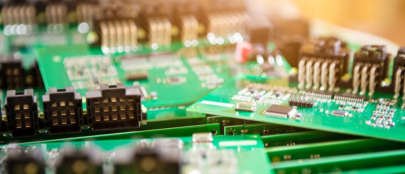
PCB Layout Strategies for High-Frequency Performance
The printed circuit board (PCB) layout is one of the most influential factors in determining how a circuit will behave at high frequencies. Here are some proven strategies:
- Layer Stackup: Use a multilayer PCB with dedicated ground and power planes to reduce loop areas and improve signal integrity.
- Trace Geometry: Maintain consistent trace width and spacing to control characteristic impedance. For differential signals, ensure traces are routed as pairs with constant separation.
- Via Management: Minimize the use of vias, as they introduce inductance and can disrupt signal flow. When necessary, use back-drilling or via stitching to mitigate these effects.
- Component Placement: Place critical components as close as possible to minimize trace lengths, especially for high-speed or sensitive analog sections.
- Return Paths: Ensure that high-frequency currents have a direct and uninterrupted return path, typically provided by a continuous ground plane beneath signal traces.
Material Selection and Its Impact on Signal Integrity
The choice of PCB materials plays a significant role in how signals propagate at high frequencies. Standard FR-4 may suffice for lower frequencies, but as speeds increase, its losses and dielectric variability can become problematic. Consider these factors:
- Dielectric Constant (Dk): Materials with a stable and low Dk, such as PTFE-based laminates, help maintain consistent impedance and reduce signal distortion.
- Loss Tangent (Df): Lower loss tangent materials minimize signal attenuation, which is crucial for maintaining signal strength over longer traces.
- Thermal Stability: High-frequency circuits often generate more heat. Materials must withstand thermal cycling without degrading performance.
For more detailed guidance on choosing the right substrate, the electronic product design pcb material selection resource provides in-depth information.
Managing Electromagnetic Interference (EMI) and Crosstalk
As frequencies rise, circuits become more susceptible to electromagnetic interference and crosstalk between adjacent traces. Effective management is essential for reliable operation:
- Shielding: Use grounded copper pours or shields around sensitive sections to block external noise and contain emissions.
- Trace Spacing: Increase the distance between parallel traces to reduce capacitive and inductive coupling.
- Guard Traces: Place grounded guard traces between high-speed lines to further isolate signals.
- Filter Components: Incorporate ferrite beads, capacitors, or common-mode chokes at strategic points to suppress unwanted frequencies.
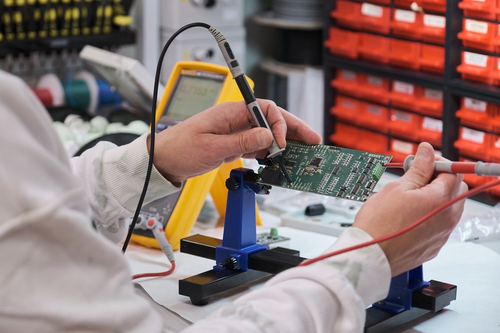
Testing and Validation of High-Frequency Designs
Even with careful planning, real-world testing is essential to verify that your design meets performance goals. Consider these steps:
- Time Domain Reflectometry (TDR): Use TDR to assess impedance discontinuities and identify problematic areas in transmission lines.
- Network Analyzers: Measure S-parameters to evaluate return loss, insertion loss, and isolation between signal paths.
- EMI Testing: Conduct pre-compliance and compliance testing to ensure your product meets regulatory standards for emissions and immunity.
- Thermal Analysis: Monitor temperature rise in critical components to prevent overheating and ensure long-term reliability.
For a comprehensive overview of the manufacturing and fabrication process for advanced electronics, this ultimate guide to creating cutting-edge electronics provides valuable background and context.
Optimizing for Manufacturability and Lifecycle
Designing for high-frequency operation is only part of the equation. Ensuring that your product can be manufactured consistently and cost-effectively is equally important. Keep these points in mind:
- Design for Assembly (DFA): Simplify layouts and minimize unique parts to reduce assembly errors and costs.
- Component Sourcing: Select components with proven high-frequency performance and reliable supply chains.
- Lifecycle Considerations: Plan for obsolescence and ensure that alternative parts are available for long-term support.
- Documentation: Maintain clear and detailed design files, test procedures, and revision histories to support troubleshooting and future updates.
If you’re interested in a deeper dive into cost analysis and lifecycle planning for electronics, the electronic product lifecycle cost analysis article is a helpful resource.
Frequently Asked Questions
What are the most common mistakes in high-frequency circuit design?
The most frequent errors include neglecting impedance matching, using poor PCB layouts with long or irregular traces, ignoring the effects of parasitics, and failing to provide adequate grounding. Overlooking EMI shielding and not validating designs through proper testing can also lead to performance issues.
How does PCB material affect high-frequency performance?
PCB material impacts signal integrity, loss, and impedance control. Materials with low and stable dielectric constants and low loss tangents are preferred for high-frequency circuits, as they reduce signal attenuation and distortion. Choosing the right substrate is crucial for maintaining performance as frequencies increase.
Why is grounding so important in high-frequency layouts?
Grounding provides a stable reference for signals and minimizes noise, crosstalk, and EMI. A continuous, low-impedance ground plane ensures that return currents follow the intended paths, reducing the risk of interference and signal degradation.