


Understanding the language used in electronics manufacturing is essential for engineers, designers, and anyone involved in bringing electronic products to life. The field is filled with specialized terms that describe processes, materials, and quality standards. Mastering this vocabulary not only improves communication but also helps avoid costly mistakes during product development and production.
This guide introduces key concepts and definitions you’ll encounter in the world of electronics fabrication terminology. Whether you’re new to the industry or looking to refresh your knowledge, these explanations will help you navigate technical discussions and documentation with confidence.
For a deeper dive into how design and integration fit into the manufacturing process, the electronic product design system integration guide offers valuable insights on system-level considerations.
Essential Terms in Electronics Manufacturing
The electronics industry uses a wide range of terms to describe the steps, materials, and quality checks involved in producing circuit boards and assemblies. Here are some of the most important words and phrases you’ll encounter:
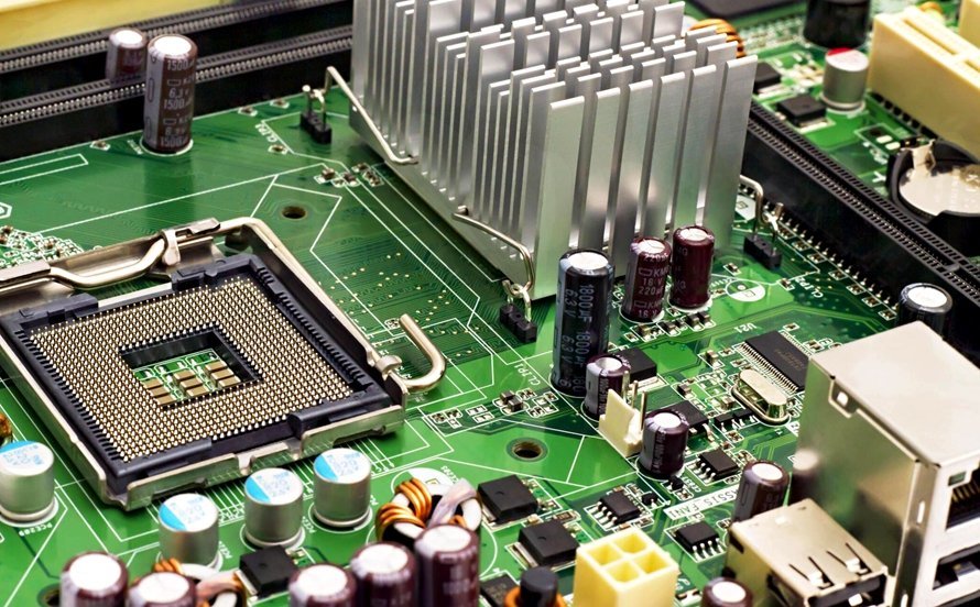
PCB (Printed Circuit Board)
A printed circuit board is the foundational platform for mounting and connecting electronic components. PCBs are typically made from fiberglass-reinforced epoxy laminate with copper traces that form the circuit. They can be single-sided, double-sided, or multilayer, depending on complexity.
Substrate
The substrate refers to the base material of a PCB or other electronic assembly. Common substrates include FR-4 (a glass-reinforced epoxy), ceramic, and flexible polymers. The choice of substrate affects thermal performance, flexibility, and cost.
Gerber Files
Gerber files are the standard digital format used to communicate PCB design data to manufacturers. These files contain information about copper layers, solder masks, silkscreen, and drill data, ensuring accurate production of the intended circuit layout.
Solder Mask
The solder mask is a protective layer applied to the PCB to prevent solder bridges and oxidation. It covers the copper traces except where components will be soldered, typically appearing as a green or other colored coating.
Silkscreen
This is the layer on a PCB where text, symbols, and component outlines are printed. The silkscreen helps with assembly and troubleshooting by labeling parts and indicating orientation.

Key Processes in Electronics Fabrication
Several manufacturing steps are crucial in transforming a design into a working electronic product. Understanding these process terms is vital for effective project management and quality control.
Etching
Etching is the process of removing unwanted copper from a PCB to form the desired circuit pattern. Chemical solutions or laser techniques are used to dissolve exposed copper after a resist layer is applied.
Drilling
This step creates holes for through-hole components and vias (connections between layers). Precision drilling ensures proper alignment and electrical connectivity.
Plating
Plating deposits a thin layer of metal, usually copper, inside drilled holes and on the board’s surface to improve conductivity and solderability. Additional plating with tin, gold, or silver may be used for specific requirements.
Surface Mount Technology (SMT)
SMT is a method of mounting components directly onto the surface of a PCB. It allows for smaller, more densely packed assemblies compared to traditional through-hole techniques. SMT has become the industry standard for most modern electronics.
Through-Hole Technology
This older assembly method involves inserting component leads into pre-drilled holes and soldering them to pads on the opposite side. Through-hole mounting is still used for components that require strong mechanical bonds or high power handling.
Common Quality and Inspection Terms
Ensuring reliability and safety in electronic products requires rigorous inspection and testing. Here are some terms related to quality assurance in electronics fabrication terminology:
AOI (Automated Optical Inspection)
AOI uses cameras and software to inspect PCBs for defects such as solder bridges, missing components, or misalignments. It is a fast, non-contact method for catching errors early in the production process.
ICT (In-Circuit Testing)
In-circuit testing checks the electrical performance of assembled PCBs by probing test points. ICT can detect open circuits, shorts, and incorrect component values, helping to ensure functional integrity.
Functional Testing
This process verifies that the finished electronic assembly performs its intended function. Functional testing may involve applying power, simulating inputs, and measuring outputs under real-world conditions.
DFM (Design for Manufacturability)
DFM is a set of guidelines aimed at making a product easier and more cost-effective to manufacture. By considering manufacturing constraints during the design phase, teams can reduce errors, speed up production, and lower costs.
Materials and Component-Related Vocabulary
Materials science plays a major role in electronics manufacturing. Here are some important terms related to the substances and parts used in assembly:
- Solder Paste: A mixture of powdered solder and flux applied to PCB pads before component placement. It melts during reflow soldering to create electrical connections.
- Flux: A chemical agent that cleans and prepares metal surfaces for soldering, improving wetting and bond strength.
- Via: A plated-through hole that connects different layers of a multilayer PCB. Vias can be through-hole, blind (connecting outer to inner layers), or buried (connecting only inner layers).
- BOM (Bill of Materials): A comprehensive list of all components, materials, and subassemblies required to build an electronic product. The BOM is essential for procurement and production planning.
- Pick and Place: An automated process where machines place surface-mount components onto a PCB with high speed and accuracy.
Advanced Concepts in Electronics Fabrication
As technology advances, new terms and techniques continue to emerge. Staying updated with the latest electronics fabrication terminology is crucial for professionals in the field. Here are a few advanced concepts:
HDI (High-Density Interconnect)
HDI refers to PCB designs with a higher density of wiring and components, often using microvias and fine lines. HDI technology enables the miniaturization of devices without sacrificing performance.
Reflow Soldering
This is the process of melting solder paste to attach surface-mount components to a PCB. The assembly passes through a controlled oven, where the solder reflows and solidifies to form reliable joints.
Stencil
A stencil is a thin metal sheet with cutouts matching the PCB pads. It is used to apply solder paste accurately before component placement.
Panelization
Panelization groups multiple PCBs into a single panel for efficient manufacturing and assembly. After processing, individual boards are separated (depanelized) for final use.
Resources for Further Learning
To expand your understanding of manufacturing concepts, consider exploring the ultimate guide to electronics manufacturing for a comprehensive overview of processes and best practices. Additionally, internal resources like the electronic product design documentation workflow and electronic product design performance testing guide provide practical guidance on documentation and testing strategies.
Frequently Asked Questions
What is the difference between SMT and through-hole assembly?
Surface mount technology (SMT) involves mounting components directly onto the surface of a PCB, allowing for higher component density and automated assembly. Through-hole assembly requires inserting component leads into drilled holes and soldering them on the opposite side, providing stronger mechanical bonds but taking up more space.
Why are Gerber files important in electronics manufacturing?
Gerber files are the industry standard for communicating PCB design data to manufacturers. They contain precise information about copper traces, solder masks, and drill holes, ensuring that the final product matches the designer’s intent.
How does automated optical inspection (AOI) improve quality?
AOI uses cameras and image processing to quickly detect defects such as missing components, solder bridges, and misalignments. This automated process helps catch errors early, reducing rework and improving overall product quality.
Conclusion
Familiarity with electronics fabrication terminology is essential for anyone involved in the design, production, or quality assurance of electronic products. By understanding the language of the industry, you can communicate more effectively, avoid misunderstandings, and contribute to successful project outcomes. As technology continues to evolve, staying current with new terms and practices will help you remain competitive in the dynamic world of electronics manufacturing.