

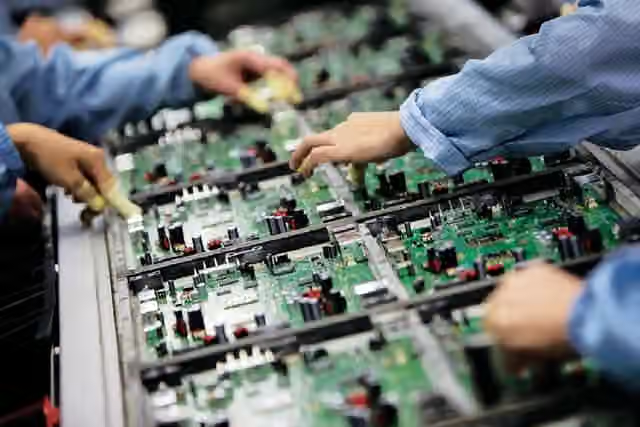
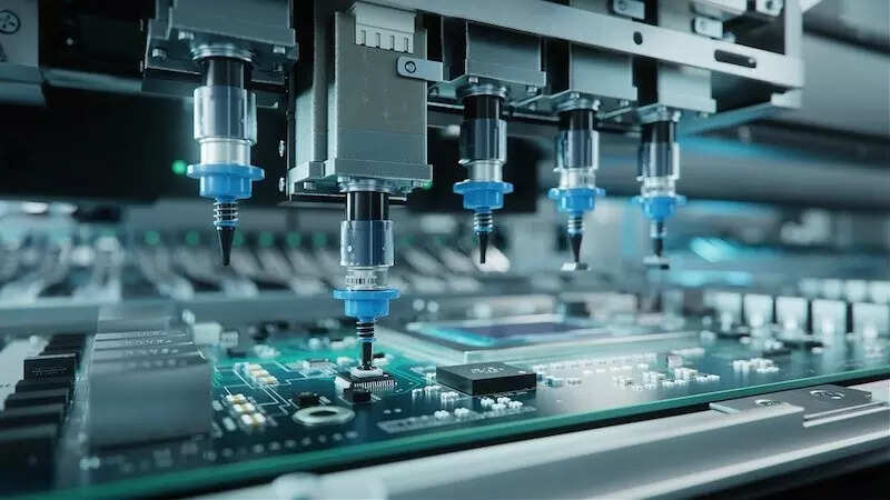
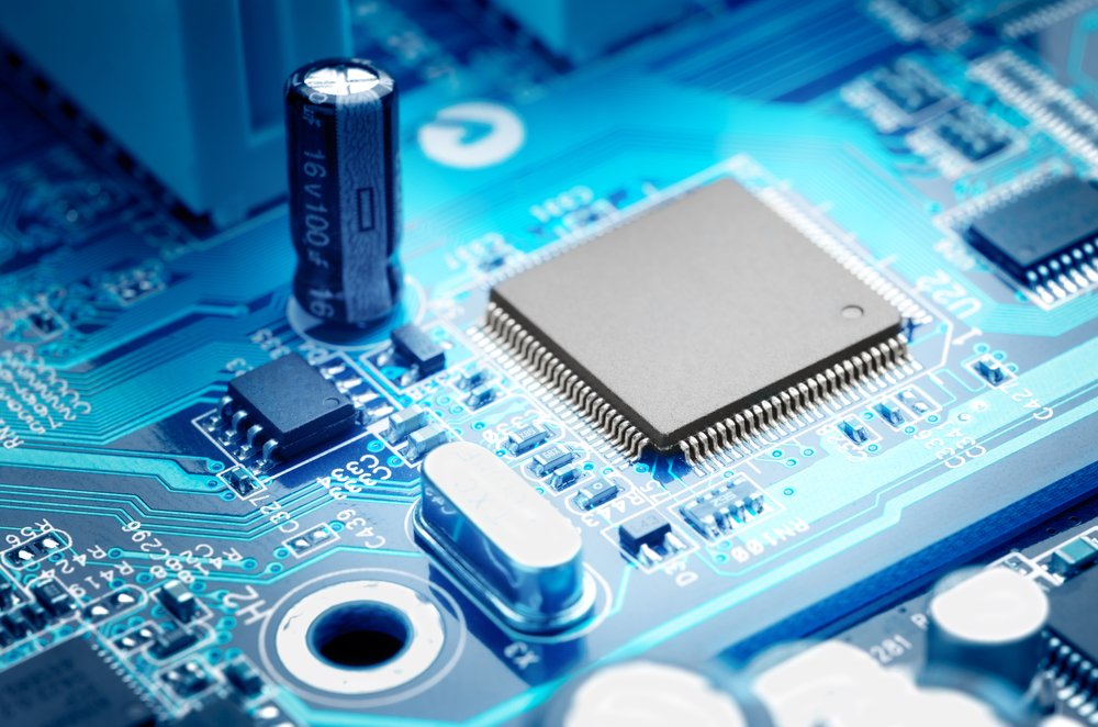
Understanding the differences between etching and deposition is essential for anyone interested in electronics manufacturing, semiconductor fabrication, or microfabrication processes. Both techniques play pivotal roles in shaping and building the intricate structures found in modern electronic devices, but they serve fundamentally different purposes. This article provides a clear, practical overview of these two core processes, their applications, and how they fit into the broader context of electronics production.
For those interested in the regulatory and procedural aspects of electronics development, you may also find value in our electronic product design safety standards comparison, which explores how safety requirements influence design and manufacturing choices.
Fundamentals of Etching and Deposition in Electronics Manufacturing
In the context of electronics fabrication, etching and deposition are two complementary processes used to create the microscopic patterns and layers that define integrated circuits, printed circuit boards (PCBs), and other microelectronic components. While both are essential, they achieve opposite outcomes:
- Etching selectively removes material from a surface to reveal desired patterns or structures.
- Deposition adds thin layers of material onto a substrate, building up the structures needed for device functionality.
These processes are repeated in sequence throughout the manufacturing workflow, allowing for the precise construction of complex electronic devices.
What Is Etching? Process, Types, and Applications
Etching is a subtractive process used to remove layers of material from a substrate, typically silicon wafers or metal films. The goal is to create specific patterns, channels, or features by eliminating unwanted material. Etching is a cornerstone of microfabrication, enabling the formation of transistors, interconnects, and other structures at the nanoscale.
Types of Etching Techniques
- Wet Etching: Uses liquid chemicals (etchants) to dissolve materials. It is generally less expensive and suitable for large-scale removal but offers less precision.
- Dry Etching: Employs gases or plasmas to remove material. This method provides greater control and is essential for creating fine, detailed features in modern microelectronics.
Key Steps in the Etching Process
- Masking: A protective layer (photoresist) is applied to define the areas to be etched.
- Etching: The exposed regions are subjected to the etchant, removing the unprotected material.
- Stripping: The mask is removed, revealing the final pattern.
Etching is used in the production of integrated circuits, MEMS devices, and PCBs. Its precision is vital for achieving the miniaturization and complexity required in today’s electronics.
Deposition: Building Layers in Microfabrication
Deposition is the process of adding thin films of material onto a substrate. These films can be conductive, insulating, or semiconducting, depending on the device requirements. Deposition is a foundational step in building up the multiple layers that make up chips, sensors, and other microdevices.
Common Deposition Methods
- Physical Vapor Deposition (PVD): Material is vaporized in a vacuum and then condensed onto the substrate. Techniques include sputtering and evaporation.
- Chemical Vapor Deposition (CVD): Chemical reactions in a gas phase produce a solid material that deposits onto the substrate. CVD is widely used for its uniformity and ability to coat complex shapes.
- Electrochemical Deposition: Involves the use of electrical current to deposit metals from a solution, commonly used for plating and creating conductive pathways.
Deposition allows for the creation of extremely thin and uniform films, which are essential for device performance and reliability.
Comparing Etching and Deposition: Key Differences and Roles
While both processes are integral to electronics manufacturing, their functions are fundamentally different. Here’s a concise comparison to clarify their roles:
| Aspect | Etching | Deposition |
|---|---|---|
| Purpose | Removes material to define patterns | Adds material to build layers |
| Direction | Subtractive | Additive |
| Common Materials | Silicon, metals, oxides | Metals, insulators, semiconductors |
| Main Techniques | Wet, dry (plasma, reactive ion) | PVD, CVD, electrochemical |
| Applications | Patterning, microstructure formation | Layer creation, coating, doping |
Understanding these distinctions helps clarify why both steps are necessary for fabricating modern electronic devices.
How Etching and Deposition Work Together in Device Fabrication
In a typical electronics manufacturing process, deposition and etching are performed in cycles. A layer is first deposited onto the wafer or substrate using one of the deposition methods. Next, photolithography is used to define the areas to be patterned, followed by etching to remove unwanted material. This sequence is repeated multiple times, gradually building up the complex, multi-layered structures found in integrated circuits and other microdevices.
For example, in semiconductor fabrication, a thin film of silicon dioxide might be deposited onto a silicon wafer. Photolithography defines the regions to be etched, and then a dry etching process removes the exposed oxide, leaving behind the desired pattern. This combination of additive and subtractive steps enables the creation of transistors, interconnects, and other essential features.
Practical Considerations: Choosing Between Etching and Deposition
The choice between etching and deposition depends on the specific requirements of the device being manufactured. Factors to consider include:
- Feature Size: Etching is critical for defining small, precise features, while deposition is used to create uniform layers.
- Material Properties: The desired electrical, mechanical, or chemical properties of the final device will influence which materials and processes are chosen.
- Process Integration: Both steps must be compatible with each other and with other processes such as photolithography and doping.
- Cost and Throughput: Wet etching and some deposition methods are faster and less expensive, but may offer less precision than dry etching or advanced CVD techniques.
Selecting the right combination of techniques is essential for achieving the required performance, reliability, and manufacturability of electronic products.
Industry Applications and Trends
These core processes are used in a wide range of industries, including:
- Semiconductor manufacturing: For integrated circuits, memory chips, and microprocessors.
- Printed circuit board (PCB) fabrication: Creating conductive pathways and mounting surfaces.
- MEMS (Micro-Electro-Mechanical Systems): Building sensors, actuators, and microfluidic devices.
- Solar cell production: Patterning and layering photovoltaic materials.
As device geometries shrink and performance demands increase, new materials and advanced process control techniques are being developed to improve both etching and deposition. For a broader look at how these methods fit into the overall electronics manufacturing workflow, see this comprehensive overview of the electronics manufacturing process.
Related Topics in Electronic Product Design
If you’re interested in how these fabrication processes impact product development, you might also explore our resources on electronic product design documentation workflow and electronic product design performance testing guide. These guides provide practical insights into managing the complexities of modern electronics projects.
Frequently Asked Questions
What is the main difference between etching and deposition?
The primary distinction is that etching removes material to create patterns or structures, while deposition adds material to build up layers on a substrate. Both are essential for manufacturing microelectronic devices, but they serve opposite functions—one is subtractive, the other additive.
Why are both etching and deposition necessary in semiconductor fabrication?
Both processes are required to construct the complex, multi-layered architecture of integrated circuits. Deposition creates the thin films needed for device operation, while etching defines the intricate patterns and features. Repeating these steps in sequence enables the precise construction of transistors, interconnects, and other critical components.
What are some common challenges with etching and deposition?
Common challenges include achieving uniformity and precision, avoiding defects, and ensuring compatibility between materials and processes. As device features become smaller, controlling the selectivity and accuracy of both etching and deposition becomes increasingly important to maintain yield and performance.
How do I learn more about electronics manufacturing processes?
For a deeper dive into the full range of steps involved in producing electronic devices, refer to this detailed guide to electronics manufacturing processes. It covers everything from raw materials to final assembly and testing.