

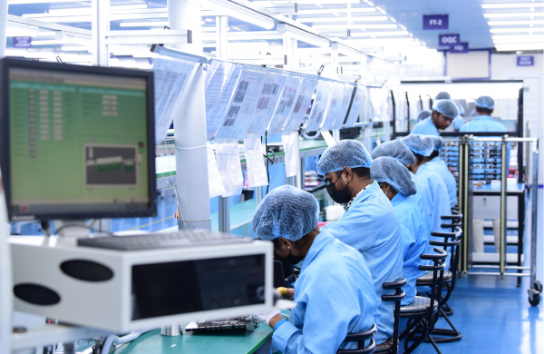
The world of electronics relies heavily on the precise and intricate process of making semiconductors. These tiny components are the backbone of modern devices, from smartphones and computers to cars and medical equipment. Understanding semiconductor fabrication basics is essential for anyone interested in electronics manufacturing, product design, or technology innovation.
At its core, the process involves transforming raw silicon wafers into highly complex integrated circuits through a series of carefully controlled steps. Each stage, from wafer preparation to final assembly, requires advanced technology and strict quality control. For those looking to deepen their knowledge of how electronic products are brought to life, exploring the fundamentals of chip manufacturing provides valuable insight.
For a deeper understanding of how these components are tested and validated after production, you may find the electronic product design performance testing guide helpful. It covers essential steps in ensuring product reliability and performance.
Key Steps in Modern Chip Manufacturing
The journey from raw materials to finished microchips involves several major stages. Each step in the semiconductor fabrication process must be performed in ultra-clean environments to prevent contamination and defects. Here’s a breakdown of the main phases:
- Wafer Preparation: High-purity silicon is sliced into thin wafers, polished, and cleaned to provide a flawless starting surface.
- Photolithography: A light-sensitive coating is applied to the wafer, and patterns are projected onto it using ultraviolet light. This defines the intricate circuit layouts.
- Etching: Chemical or plasma etching removes unwanted material, leaving behind the desired circuit patterns.
- Doping: Specific regions are infused with impurities to alter the electrical properties of the silicon, creating p-type and n-type areas.
- Deposition: Thin layers of materials such as metals or insulators are deposited onto the wafer to form connections and insulation.
- Testing and Dicing: Completed wafers are tested for defects, then cut into individual chips (dies).
- Packaging and Assembly: Each die is mounted in a protective package and connected to external pins or pads for integration into electronic devices.
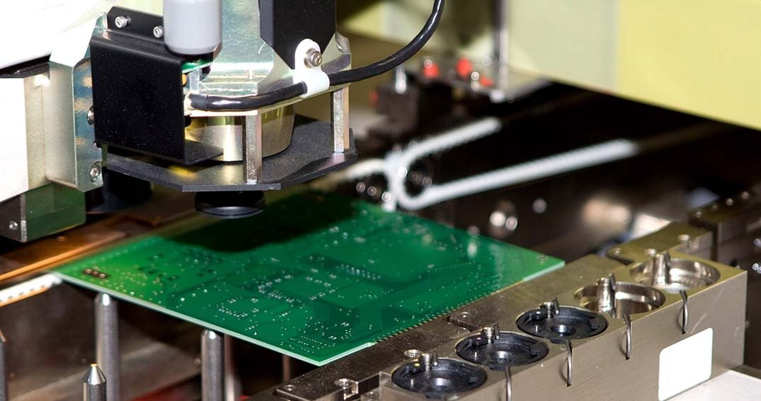
Cleanroom Environments and Contamination Control
One of the most critical aspects of chip production is maintaining an ultra-clean environment. Even microscopic particles can ruin a wafer, causing defects that render chips unusable. Cleanrooms are classified by the number of particles per cubic meter, with the most advanced facilities reaching ISO Class 1 or 2.
Workers wear specialized suits, and air is constantly filtered to remove dust and contaminants. Equipment is designed to minimize particle generation, and strict protocols are followed for every movement and process. This level of control is necessary to achieve the high yields and reliability demanded by modern electronics.
Materials and Technologies Used in Fabrication
While silicon remains the primary material for most integrated circuits, other substances play vital roles in the process. Metals like aluminum and copper are used for wiring, while insulators such as silicon dioxide separate different layers. Advanced processes may also use compound semiconductors (like gallium arsenide) for specialized applications.
The choice of materials and fabrication techniques can significantly impact performance, power consumption, and cost. For example, the shift to copper interconnects in recent decades enabled faster and more efficient chips. Similarly, new lithography methods, such as extreme ultraviolet (EUV), allow for smaller and more complex features on each chip.
Assembly and Testing in Semiconductor Manufacturing
After fabrication, each chip must be assembled and thoroughly tested before it can be used in electronic products. Assembly involves attaching the chip to a substrate, connecting it to external leads, and encapsulating it in a protective package. This stage is crucial for durability and integration into circuit boards.
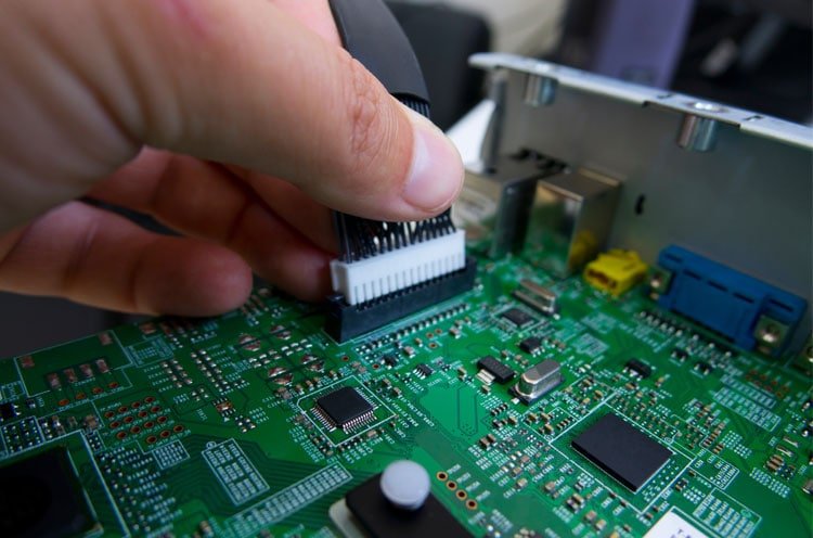
Testing ensures that each device meets strict specifications for performance and reliability. Automated systems check for electrical faults, speed, power consumption, and other parameters. Only chips that pass all tests move on to final integration. For more on the importance of material choices in assembly, the electronic product design pcb material selection guide provides additional insights.
Challenges and Innovations in Chip Production
The field of semiconductor fabrication is constantly evolving. As demand for smaller, faster, and more energy-efficient chips grows, manufacturers face new challenges. Shrinking feature sizes increases the risk of defects and requires ever-more precise equipment. The cost of building and maintaining fabrication plants (fabs) has also risen dramatically.
To address these challenges, the industry invests heavily in research and development. Innovations like 3D stacking, advanced packaging, and new materials are pushing the boundaries of what’s possible. Collaboration across the supply chain, from raw material suppliers to assembly partners, is essential for success.
For those interested in hands-on assembly techniques and project work, resources such as a beginner’s guide to manual electronics assembly can provide practical tips and foundational knowledge.
Applications and Impact of Semiconductor Devices
The products of chip manufacturing power nearly every aspect of modern life. Microprocessors, memory chips, sensors, and power devices are found in consumer electronics, industrial equipment, automotive systems, and medical devices. The reliability and performance of these components directly influence the capabilities of end products.
As new applications emerge—such as artificial intelligence, 5G communications, and the Internet of Things—the demand for advanced semiconductors will only increase. Understanding the basics of how these components are made helps engineers, designers, and business leaders make informed decisions throughout the product lifecycle.
For a broader perspective on managing costs and optimizing product development, the electronic product lifecycle cost analysis guide offers valuable strategies.
Frequently Asked Questions
What is the most important step in chip manufacturing?
Every stage in the process is critical, but photolithography is often considered the most technically demanding. It defines the patterns that form the circuits and determines how small and complex a chip can be.
Why are cleanrooms necessary in semiconductor fabrication?
Cleanrooms prevent contamination by dust and particles, which can cause defects in microchips. Even a single microscopic particle can ruin an entire wafer, so strict cleanliness is essential for high yields and reliable products.
How do material choices affect chip performance?
The materials used for wiring, insulation, and the semiconductor itself influence speed, power consumption, and durability. Advances in materials science have enabled faster and more efficient chips, supporting the ongoing evolution of electronic devices.
