

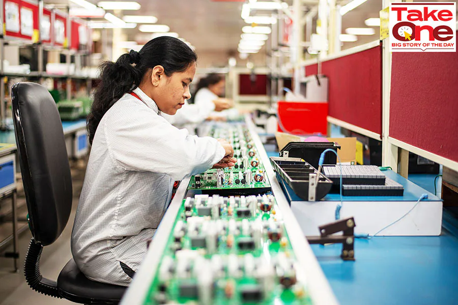
Photolithography is a foundational process in semiconductor manufacturing and microfabrication. It enables the creation of intricate patterns on silicon wafers, which are essential for producing integrated circuits and microchips. This technique uses light to transfer geometric patterns from a photomask onto a light-sensitive chemical photoresist layer, allowing for the precise etching and layering needed in modern electronics.
Understanding how this process works is crucial for anyone interested in electronics manufacturing, microengineering, or the evolution of computing technology. For those involved in developing new electronic products, mastering the basics of photolithography can significantly impact design decisions and manufacturing outcomes. If you are looking to deepen your knowledge of how electronic systems come together, the electronic product design system integration guide provides valuable context on how photolithography fits into the broader product development workflow.
What Is Photolithography and Why Is It Important?
At its core, photolithography is a process that uses light to define patterns on a substrate, typically a silicon wafer. The patterns created are used to build the tiny transistors, wires, and other components that make up integrated circuits. This technique is vital because it allows for the mass production of highly complex and miniaturized electronic devices, from smartphones to advanced computing systems.
The ability to produce smaller and more precise features directly impacts the performance, speed, and energy efficiency of electronic devices. As the demand for more powerful and compact technology grows, advances in photolithography continue to push the boundaries of what is possible in semiconductor fabrication.
The Photolithography Process Step by Step
The photolithography workflow involves several carefully controlled steps, each critical to achieving the desired pattern accuracy and resolution. Here’s a breakdown of the typical process:
- Wafer Cleaning: The silicon wafer is thoroughly cleaned to remove any contaminants that could interfere with pattern formation.
- Photoresist Application: A thin layer of photoresist, a light-sensitive polymer, is evenly coated onto the wafer’s surface.
- Soft Baking: The wafer is gently heated to evaporate solvents from the photoresist, improving its adhesion and uniformity.
- Mask Alignment and Exposure: A photomask containing the desired circuit pattern is aligned over the wafer. Ultraviolet (UV) light is then shone through the mask, exposing specific areas of the photoresist.
- Development: The wafer is immersed in a developer solution, which removes either the exposed or unexposed areas of the photoresist, depending on whether a positive or negative resist is used.
- Etching: With the patterned photoresist acting as a protective layer, the wafer undergoes etching to remove material from the exposed regions, transferring the pattern onto the underlying substrate.
- Photoresist Removal: The remaining photoresist is stripped away, leaving behind the patterned wafer ready for subsequent processing steps.
Types of Photolithography Techniques
Several variations of photolithography have been developed to address the need for smaller feature sizes and higher resolution. The main types include:
- Contact Printing: The photomask is placed in direct contact with the wafer. While simple, this method can cause mask damage and is less suitable for very fine features.
- Proximity Printing: The mask is held slightly above the wafer, reducing mask wear but sacrificing some resolution due to light diffraction.
- Projection Printing: Lenses project the mask image onto the wafer without direct contact. This is the most advanced and widely used method, enabling the production of extremely small features.
Within projection printing, deep ultraviolet (DUV) and extreme ultraviolet (EUV) lithography have become essential for manufacturing the latest generations of microchips. These techniques use shorter wavelengths of light to achieve higher resolution and pack more transistors onto a single chip.
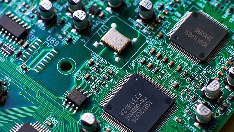
Key Materials Used in Photolithography
The success of the photolithography process relies on several specialized materials:
- Photoresists: Light-sensitive polymers that change their solubility when exposed to UV light. Positive resists become soluble where exposed, while negative resists become insoluble.
- Photomasks: Plates made of glass or quartz with opaque patterns that define the circuit layout.
- Developers: Chemical solutions that selectively remove parts of the photoresist after exposure.
- Etchants: Chemicals or plasmas used to remove exposed areas of the wafer, transferring the pattern from the resist to the substrate.
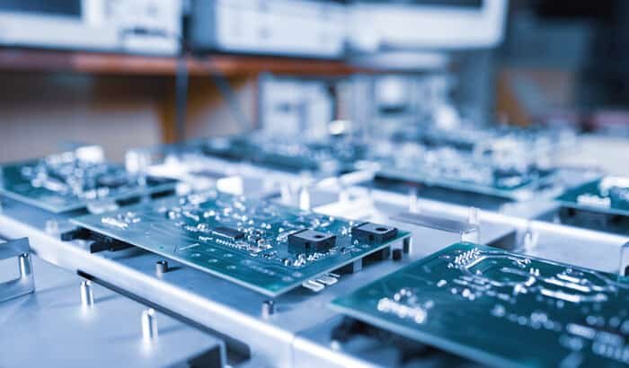
Applications of Photolithography in Modern Electronics
Photolithography is indispensable in the production of:
- Microprocessors and memory chips for computers, smartphones, and servers
- Microelectromechanical systems (MEMS) used in sensors and actuators
- Display technologies such as LCD and OLED panels
- Photonic devices for optical communications
Its precision and scalability have enabled the exponential growth of computing power and the miniaturization of devices. As a result, photolithography remains a key driver of innovation in the electronics industry.
Challenges and Advances in Photolithography
As feature sizes on chips continue to shrink, photolithography faces several technical challenges:
- Resolution Limits: The wavelength of light used in exposure sets a fundamental limit on the smallest achievable features. EUV lithography, using 13.5 nm light, is currently pushing these boundaries.
- Mask Defects: Any imperfection on the photomask can be transferred to every chip, making mask quality and inspection critical.
- Process Complexity: As circuits become more intricate, the number of photolithography steps increases, raising costs and the risk of defects.
To address these issues, researchers and manufacturers are exploring new materials, multi-patterning techniques, and alternative approaches such as nanoimprint lithography. For a deeper dive into the entire semiconductor manufacturing process, the ultimate guide to creating cutting-edge electronics provides comprehensive insights.
Photolithography’s Role in Product Development and Testing
For engineers and product developers, understanding photolithography is essential not only for fabrication but also for system integration and testing. The patterns defined during this process affect everything from circuit performance to reliability and safety standards. If you are interested in how these patterns are validated and tested, the electronic product design performance testing guide offers practical information on ensuring quality and compliance in electronic products.
Frequently Asked Questions
What is the difference between positive and negative photoresist?
Positive photoresist becomes soluble in the developer solution where it has been exposed to light, so the exposed areas are removed. Negative photoresist, on the other hand, becomes insoluble where exposed, so the unexposed areas are washed away. The choice between the two depends on the desired pattern and process requirements.
How does photolithography impact the performance of electronic devices?
The precision and resolution of photolithography determine how small and closely packed the features on a chip can be. Smaller features allow for more transistors per chip, which leads to faster, more efficient, and more powerful electronic devices.
Are there alternatives to photolithography for microfabrication?
Yes, alternatives such as electron beam lithography, nanoimprint lithography, and focused ion beam lithography exist. However, photolithography remains the most widely used technique for high-volume manufacturing due to its speed, scalability, and cost-effectiveness.