

Designing a Printed Circuit Board (PCB) requires precision and planning, especially when it comes to PCB stackup optimization. Optimizing your stackup not only enhances the board’s performance but also reduces costs in production. Whether you’re an exporter or importer in the electronics sector, understanding the nuances of PCB design can improve your operational efficiency and product quality. This comprehensive guide will walk you through the critical aspects of stackup optimization.

Why is PCB Stackup Important?
A well-optimized PCB stackup minimizes electromagnetic interference, maintains signal integrity, and improves thermal management. Effective stackup design is crucial for custom electronics manufacturing and creates a foundation for high-performance electronics.
Components of a PCB Stackup
Stackup primarily consists of thin layers of copper and dielectric material. By optimizing these layers, you can control impedance and ensure that signals travel efficiently from one layer to the next. Each layer plays an essential role in the circuit’s performance.
Benefits of Optimized Stackup
Optimizing the stackup affects thermal and signal management, which impacts the lifespan and reliability of a PCB. Companies involved in export and import can ensure that the electronics they deal in are of high quality, reliable, and meet international standards.
Understanding Layer Configuration
Configuring your layers correctly is one aspect of stackup optimization. The right configuration can affect everything from the board’s electrical characteristics to its manufacturing yield. For exporters and importers, a precise configuration ensures compliance and functionality in various global markets.
Single-layer and Multi-layer PCBs
While single-layer PCBs are simpler and cheaper, multi-layer boards provide enhanced capabilities, including complex signal routing and improved performance. The choice between them depends on the complexity and application needs of your electronics.
Material Considerations in Stackup
Choosing the right materials is essential for achieving the desired electrical characteristics. Manufacturers often depend on core and pre-preg materials to create the dielectric layers needed for their circuits. External resources provide further insights into how to best use these materials in prototyping.
High-frequency Material Choices
For high-speed applications, materials with low loss characteristics prevent signal degradation. Designs using high-frequency materials are more common in telecommunications and computing industries.
Tackling Impedance Control
Impedance control is vital for maintaining the integrity of high-speed signals. Proper stackup optimization involves setting up controlled impedance lines which are crucial for modern electronics.
Stripline and Microstrip Configurations
These circuit path configurations help ensure consistent impedance, essential for high-speed circuits.
Thermal Management in PCB Design
Effective thermal management is vital in PCB stackup optimization to prevent overheating and ensure longevity. Proper design can dissipate heat efficiently, maintaining the efficiency of the board.
Thermal Vias and Conductive Paths
Utilizing thermal vias and conductive paths allows for better heat dissipation, which supports overall circuit longevity and reliability.
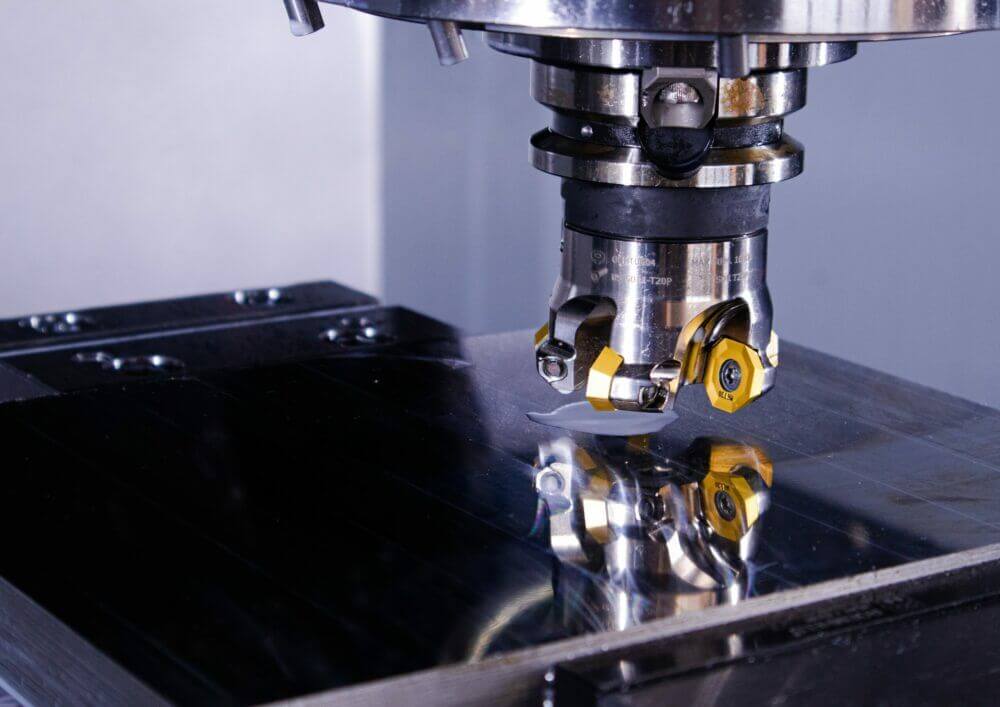
Tooling and Prototyping Techniques for Optimization
Various CAD tools and prototyping techniques are employed to design the most efficient stackup. Effective usage of these tools is critical in circuit simulation, helping to create electronic components with precision.
Circuit Simulation Tools
Tools like EDA (Electronic Design Automation) help ensure stackup designs are optimized for best performance before moving to production stages. Simulations help in identifying potential flaws in the stackup.
Cost Implications of Stackup Design
Optimized PCBs lower costs by improving yield and reducing material waste. Understanding how to design stackups effectively can be a critical cost-saving strategy for exporters and importers.
Balancing Cost and Performance
Striking a balance between cost and performance ensures you maintain quality without exceeding budget constraints.
Regulatory and Compliance Considerations
Adhering to regulations and standards both locally and internationally is crucial. Well-engineered PCBs must comply with these to be viable in the global market, which is important for exporters and importers alike.
International Standards
There are several standards like IPC that guide PCB design and stackup. Meeting these standards ensures your electronics are globally competitive.
Conclusion: The Future of PCB Stackup Optimization
Advancements in materials and computer-aided design tools continue to evolve the landscape of PCB design. For those involved in export and import, embracing these changes and optimizing their stackups will lay the groundwork for success in the global electronics market.
Staying Ahead with Technology
For ongoing success, staying informed about advances in PCB technology and incorporating them into your production cycle will be pivotal.

FAQs
What is PCB stackup optimization?
It involves designing the layers of a PCB to optimize performance, reduce interference, and improve thermal management. This helps in producing high-quality electronics efficiently.
Why is layer material selection important?
Choosing the right materials can affect the electrical performance, thermal management, and manufacturing cost of the circuit.
How does impedance affect PCB performance?
Properly controlled impedance ensures that signals remain stable, reducing noise and increasing the reliability of the circuit.