

The demand for smaller, lighter, and more efficient electronic devices continues to shape the future of technology. From smartphones and wearables to medical implants and industrial sensors, the push for compactness drives innovation across the electronics sector. Electronics miniaturization techniques are at the heart of this evolution, enabling manufacturers to pack more functionality into ever-tinier packages without sacrificing performance or reliability.
As products become more sophisticated, understanding the methods and challenges behind shrinking electronic components is essential for engineers, designers, and anyone involved in product development. This article explores the core strategies, manufacturing processes, and practical considerations that make miniaturized electronics possible.
For those interested in the broader process of bringing a compact device to market, the electronic product design system integration guide provides a comprehensive overview of system-level considerations.
Key Drivers Behind Compact Electronics
The push for miniaturization is not just about aesthetics or convenience. Several practical factors motivate the industry to pursue smaller electronic assemblies:
- Portability: Smaller devices are easier to carry and integrate into daily life, fueling the growth of wearables and mobile gadgets.
- Functionality: Miniaturization allows for more features to be included in a single product, enhancing user experience.
- Energy Efficiency: Reduced size often means lower power consumption, which is critical for battery-powered applications.
- Cost Reduction: Using less material and space can lower manufacturing and shipping costs.
- Medical and Industrial Applications: Many fields require electronics that fit into tight spaces, such as implants or embedded sensors.
Core Approaches to Electronics Miniaturization
Achieving smaller, more capable electronics involves a combination of design, material science, and advanced manufacturing. Here are some of the most widely used electronics miniaturization techniques:
Surface Mount Technology (SMT)
SMT revolutionized assembly by allowing components to be mounted directly onto the surface of printed circuit boards (PCBs), eliminating the need for through-hole leads. This approach supports higher component density and enables double-sided board assembly, making it a cornerstone of modern miniaturization.
Multi-Layer and High-Density Interconnect (HDI) PCBs
By stacking multiple PCB layers and using microvias, HDI technology allows for more complex routing and higher component density. This is essential for advanced devices such as smartphones, where space is at a premium.
System-in-Package (SiP) and Chip-Scale Packaging (CSP)
SiP integrates multiple integrated circuits (ICs) and passive components into a single package, reducing the overall footprint. CSP goes even further, shrinking the package size to nearly that of the chip itself. These packaging innovations are key for applications where every millimeter counts.
Microelectromechanical Systems (MEMS)
MEMS technology enables the integration of mechanical elements, sensors, actuators, and electronics on a single silicon chip. This approach is widely used in accelerometers, gyroscopes, and pressure sensors found in mobile devices and medical equipment.
Design Strategies for Compact Devices
Beyond hardware, thoughtful design is essential for successful miniaturization. Here are some strategies engineers use to optimize space and performance:
- Component Selection: Choosing smaller or integrated components, such as combined microcontrollers with built-in peripherals, helps save board space.
- 3D Integration: Stacking components vertically, rather than spreading them out, maximizes volume efficiency.
- Flexible and Rigid-Flex PCBs: These allow circuits to bend and fold, enabling creative layouts in tight enclosures.
- Thermal Management: As density increases, so does heat. Careful placement and the use of thermal vias or heat spreaders are crucial.
- Signal Integrity: High-speed signals in close quarters require careful routing and shielding to prevent interference.
Manufacturing Challenges and Solutions
Shrinking electronics introduces new production hurdles. Manufacturers must address issues such as:
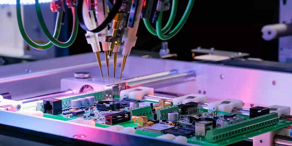
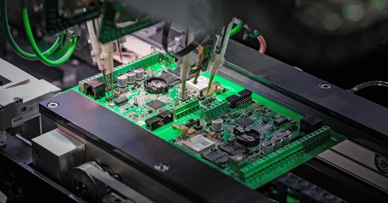
- Precision Assembly: Placing tiny components accurately demands advanced pick-and-place machines and inspection systems.
- Quality Control: Detecting defects at miniature scales requires high-resolution imaging and automated optical inspection (AOI).
- Testing: Miniaturized products may need specialized fixtures or non-contact testing methods to verify performance.
- Material Constraints: Thinner boards and smaller traces can be more fragile, requiring careful handling and robust design.
For a deeper look at the production side, the electronics manufacturing process overview explains how these challenges are managed from prototyping to mass production.
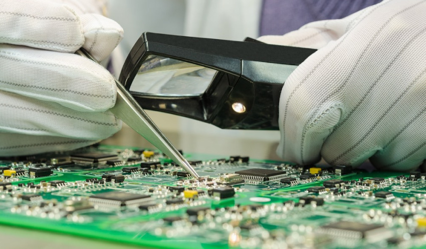
Testing and Reliability for Miniaturized Electronics
As devices shrink, ensuring reliability becomes more complex. Smaller components can be more sensitive to environmental stress, and higher densities can exacerbate issues like overheating or signal crosstalk. Rigorous testing is essential to guarantee long-term performance.
For guidance on evaluating compact products, the electronic product design performance testing guide outlines best practices for verifying function and durability.
Future Trends in Electronics Miniaturization
Innovation in this area continues at a rapid pace. Some emerging trends include:
- Advanced Materials: The use of new substrates, such as ceramics or flexible polymers, supports even smaller and more robust assemblies.
- 3D Printing: Additive manufacturing is enabling the creation of complex, miniaturized structures that were previously impossible with traditional methods.
- Nanotechnology: Incorporating nanoscale components and materials promises further reductions in size and improvements in efficiency.
- Artificial Intelligence (AI): AI-driven design tools help optimize layouts and predict potential issues in densely packed circuits.
FAQ
What are the main benefits of miniaturizing electronic devices?
The primary advantages include increased portability, greater functionality in a smaller form factor, improved energy efficiency, and reduced manufacturing costs. Miniaturized devices also enable new applications in fields like healthcare, where compactness is crucial.
Which manufacturing techniques are most important for compact electronics?
Surface mount technology, multi-layer and HDI PCBs, system-in-package, and MEMS are among the most significant. Each technique addresses different aspects of reducing size while maintaining or enhancing performance.
How do engineers ensure reliability in miniaturized products?
Reliability is achieved through careful design, rigorous testing, and the use of high-quality materials. Engineers focus on thermal management, signal integrity, and robust assembly processes to prevent failures in dense, compact assemblies.
Conclusion
The journey toward ever-smaller electronics is driven by both consumer demand and technological advancements. By leveraging a combination of electronics miniaturization techniques, innovative design strategies, and precise manufacturing, engineers are able to deliver powerful, reliable devices that fit into the palm of your hand—or even smaller. As new materials and methods emerge, the possibilities for compact electronics will only continue to expand.