

In today’s fast-paced technological world, the demand for custom PCB enclosures is ever-growing. Whether youre a seasoned exporter or an innovative importer, understanding the nuances of these enclosures is essential. Tailoring a PCB enclosure to specific requirements can mean the difference between a successful product launch and a flawed design. This guide delves into the importance of customized solutions and how they cater to the unique needs of electronics. In the following sections, we will explore what makes custom solutions advantageous, the materials used, and the impact of technology on their development.

The Importance of Custom PCB Enclosures
Custom PCB enclosures serve as protective shells that guard the intricate circuits within electronic devices. These enclosures not only protect the circuits from dust and moisture but also enhance their aesthetic appeal. As technology evolves, the demand for enclosures that provide such protection while accommodating innovative designs grows. By customizing these enclosures, businesses ensure that their products meet specific functional and aesthetic requirements, thus improving customer satisfaction and potentially increasing their market reach.
Types of Materials Used
Metal Enclosures
Metal is a popular choice for PCB enclosures due to its durability and high strength. Aluminum and stainless steel are commonly used metals that offer excellent protection against impact and corrosion. They are ideal for environments where electronic components may encounter challenging conditions.
Plastic Enclosures
Plastic enclosures are lightweight and cost-effective. They provide electrical insulation and are available in various shapes and colors, giving designers the flexibility to create appealing and functional enclosure solutions. This versatility makes plastic a leading choice for many consumer electronics.
Composite Materials
For applications requiring a combination of strength and lightweight properties, composite materials are often used. These materials offer enhanced durability and thermal management, making them suitable for advanced electronics.
The Design Process
Creating a custom PCB enclosure involves a detailed design process that incorporates client requirements, technical specifications, and aesthetic preferences. Designers use advanced software tools to create models that help visualize the final product. Once a design is approved, prototypes are developed to test the enclosure’s fit and finish.
Technological Advancements
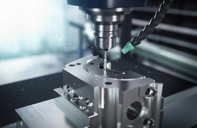
With the advent of modern manufacturing technologies, customizing PCB enclosures has become more accessible. Techniques such as 3D printing and CNC machining enable the production of complex designs with ease. These technologies streamline the development process, reduce production costs, and allow for rapid prototyping, ensuring products are brought to market swiftly.
Applications Across Industries
Custom PCB enclosures are used in an array of industries, from consumer electronics to industrial machines. Each industry demands specific features, such as heightened durability for industrial applications or sleek designs for consumer products.
Environmental Considerations
As the electronics industry strives for sustainability, more companies are opting for eco-friendly materials and processes in their enclosure design. Utilizing recyclable materials and minimizing waste in production are becoming priorities as businesses seek to reduce their environmental impact.
Challenges in Customization
While customization offers many benefits, it also poses challenges, including increased cost and longer development times. However, investing in a well-designed enclosure can result in significant savings in the long run by reducing the need for subsequent modifications and enhancing product longevity.
Choosing a Manufacturing Partner
Selecting the right manufacturing partner is critical when creating custom PCB enclosures. It’s important to collaborate with a manufacturer experienced in the specific technology and materials required for your project. Furthermore, a reliable partner will provide insights into cost-saving strategies and innovative solutions.
Cost Implications
The cost of custom enclosures can vary significantly based on materials, design complexity, and production volume. While custom options may initially be more expensive than standard solutions, the long-term benefits of tailored design often justify the price.
Quality Assurance
Ensuring quality is paramount in manufacturing custom PCB enclosures. Rigorous testing processes help identify any potential issues before products reach the market, safeguarding against costly recalls and customer dissatisfaction.
Future Trends
The future of custom enclosures lies in increased adaptation to emerging technologies such as IoT devices and smart applications. These trends demand even more personalized solutions to accommodate their unique needs.

FAQs on Custom PCB Enclosures
What are custom PCB enclosures?
Custom PCB enclosures are specially designed cases that protect and house printed circuit boards. These designs are tailored to meet the specific requirements of a product for functionality and appearance.
Why are custom enclosures better than standard ones?
Custom enclosures are preferred when unique design specifications are required. They ensure proper fit and protection for the components, enhancing the device’s performance and lifespan.
How can I find the right materials for my enclosure?
Choosing the right material depends on the intended use, budget, and environmental factors. Its beneficial to consult with experienced manufacturers to select the most suitable materials for your project.
For more insights on electronic manufacturing trends, visit circuit simulation tools and explore the evolving landscape of the industry through sustainable practices at sustainable electronics.
To further enhance your knowledge, you can explore additional resources on this topic at PCB prototyping and discover how these practices are shaping the future of electronics.