

Developing a successful electronic device requires a structured approach that takes an idea from concept to reality. Understanding the electronic product design workflow is essential for engineers, entrepreneurs, and businesses aiming to bring innovative solutions to market efficiently and cost-effectively. This guide breaks down the key phases, highlights best practices, and provides practical insights for navigating each stage of the process.
For those interested in a deeper dive into the steps involved, the electronic product design process steps article offers a detailed breakdown of each phase and their unique challenges.
Key Phases in the Development Journey
The journey from an initial idea to a finished electronic product involves several critical stages. Each phase builds upon the previous one, ensuring that the final device meets technical, functional, and market requirements. Below, we outline the main steps that form the backbone of a robust electronic product design workflow.
1. Conceptualization and Requirement Analysis
Every successful project begins with a clear understanding of the problem to be solved. During this phase, teams define the product’s purpose, target audience, and essential features. Key activities include:
- Market research to identify user needs and competitor offerings
- Defining technical and functional requirements
- Establishing project goals, timelines, and budget constraints
A thorough requirement analysis sets the stage for effective planning and reduces the risk of costly changes later in the process.
2. System Architecture and Design Planning
With requirements in place, the next step is to outline the system architecture. This involves selecting the right technologies, components, and design methodologies. Teams create block diagrams, define interfaces, and decide on hardware-software partitioning.
At this stage, it’s crucial to consider scalability, manufacturability, and compliance with industry standards. Early design decisions can have a significant impact on cost, performance, and future upgrades.

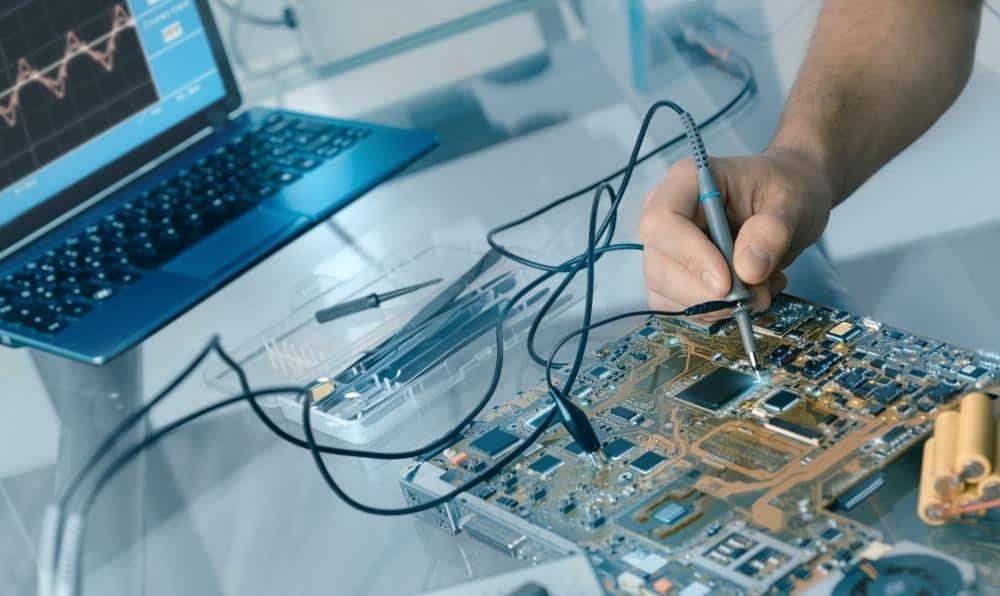
3. Schematic Capture and PCB Layout
Once the system architecture is defined, engineers move on to schematic capture—translating the conceptual design into detailed circuit diagrams. This is followed by PCB (Printed Circuit Board) layout, where the physical arrangement of components and routing of electrical connections are finalized.
- Component selection and placement
- Signal integrity and power distribution considerations
- Design for manufacturability and testability
Tools such as EDA (Electronic Design Automation) software are essential for this phase, enabling precise and efficient design iterations.
Prototyping and Validation Steps
Building and testing prototypes is a cornerstone of any electronic product design workflow. Prototyping allows teams to verify that the design meets functional requirements and to identify potential issues before moving to mass production.
4. Prototype Development
During this stage, physical prototypes are assembled using the finalized PCB layout and selected components. This hands-on phase provides valuable insights into the product’s real-world performance.
- Assembly of initial prototypes (breadboards, development kits, or custom PCBs)
- Firmware and software integration
- Basic functional and safety testing
For a comprehensive overview of this phase, the electronic prototyping process guide offers step-by-step instructions and tips for effective prototyping.
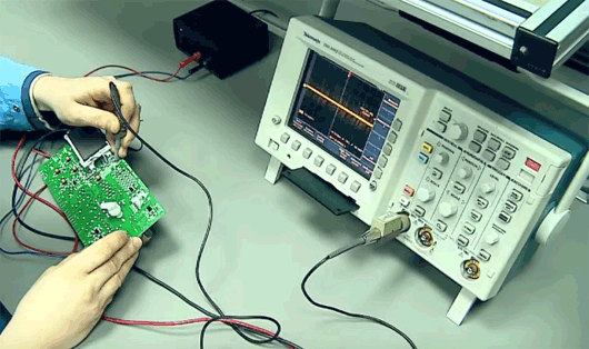
5. Testing, Iteration, and Refinement
No prototype is perfect on the first try. Rigorous testing is performed to evaluate performance, reliability, and compliance with regulatory standards. Common activities include:
- Functional, environmental, and stress testing
- Identifying and correcting design flaws
- Iterating on hardware and software as needed
This iterative approach ensures that the final product is robust and ready for real-world use.
Transitioning to Production and Market Launch
After successful prototyping and validation, attention shifts to preparing for manufacturing and launching the product. This phase is critical for ensuring scalability, quality, and cost-effectiveness.
6. Design for Manufacturing (DFM) and Compliance
Before mass production, the design is reviewed and optimized for manufacturability. This includes:
- Minimizing assembly complexity and production costs
- Ensuring compatibility with automated assembly processes
- Meeting regulatory and safety standards (such as CE, FCC, RoHS)
Collaboration with manufacturing partners at this stage helps identify potential bottlenecks and ensures a smooth production ramp-up.
7. Mass Production and Quality Assurance
With DFM completed, the product moves into full-scale manufacturing. Quality assurance processes are implemented to maintain consistency and reliability across all units. Key considerations include:
- Establishing clear quality control protocols
- Implementing traceability for components and assemblies
- Continuous monitoring and feedback loops for ongoing improvement
Effective quality management reduces the risk of defects and enhances customer satisfaction.
8. Product Launch and Post-Launch Support
The final step is launching the product to the market. This involves coordinating logistics, marketing, and distribution channels. Post-launch, it’s important to provide customer support, gather feedback, and plan for future updates or iterations.
For more information on the broader field, you can explore a comprehensive overview of electronic product design and its importance in today’s technology landscape.
Best Practices for a Streamlined Design Process
Navigating the electronic product design workflow efficiently requires attention to detail and proactive planning. Here are some best practices to keep projects on track:
- Early risk assessment: Identify technical and market risks at the outset to avoid surprises later.
- Cross-functional collaboration: Involve stakeholders from engineering, manufacturing, and marketing early in the process.
- Iterative prototyping: Embrace rapid prototyping and testing to catch issues early and refine the design.
- Documentation: Maintain thorough records of design decisions, test results, and changes for future reference and compliance.
- Scalability: Design with future upgrades and volume production in mind.
Leveraging these strategies helps teams reduce costs, accelerate time-to-market, and deliver high-quality products that meet user expectations.
Frequently Asked Questions
What is the typical timeline for an electronic device development project?
The duration varies depending on complexity, but most projects take anywhere from several months to over a year. Factors such as design complexity, regulatory requirements, and the number of prototype iterations can significantly influence the timeline.
How important is prototyping in the design workflow?
Prototyping is essential for verifying design assumptions, testing functionality, and identifying issues before mass production. It allows teams to make informed decisions and avoid costly mistakes later in the process.
What are the main challenges in bringing an electronic product to market?
Common challenges include managing design changes, ensuring regulatory compliance, controlling production costs, and maintaining quality. Effective planning, thorough testing, and strong collaboration with manufacturing partners can help overcome these hurdles.
For additional insights into related services and benefits, consider reading about benefits of electronic product design services and how expert support can streamline your next project.