

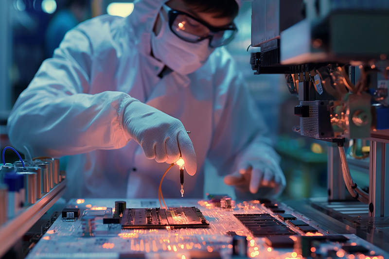
Printed circuit boards (PCBs) are the backbone of modern electronics, enabling the compact and reliable connection of components in everything from smartphones to industrial machinery. One of the most crucial steps in PCB manufacturing is etching, a process that defines the intricate copper pathways on the board. For anyone interested in electronics fabrication, understanding how etching works is essential. This guide offers a clear, step-by-step explanation of the entire procedure, its significance, and the best practices for achieving precise results.
If you’re curious about how etching fits into the broader context of electronics production, you may also find value in this detailed guide on how electronics are manufactured, which covers each stage from prototyping to final assembly.
Understanding the Basics of PCB Etching
At its core, PCB etching is the process of selectively removing unwanted copper from a laminated board to leave behind the desired circuit pattern. This is typically achieved through chemical or, less commonly, mechanical means. The result is a board with copper traces that connect various electronic components according to the circuit design.
The etching stage follows the initial steps of substrate preparation and photoresist application, and it is critical for ensuring the accuracy and reliability of the final product. Mistakes during etching can lead to short circuits, open circuits, or unreliable connections, so precision and control are paramount.
Key Steps in the PCB Etching Workflow
The PCB etching process explained step by step helps demystify how raw copper-clad boards are transformed into functional circuit boards. Here’s a breakdown of the main stages:
- Design Transfer: The desired circuit pattern is transferred onto the copper-clad board, usually through a photoresist layer that is exposed to UV light using a mask or film.
- Development: The board is developed in a solution that removes unexposed photoresist, leaving only the areas to be protected during etching.
- Chemical Etching: The board is submerged in an etchant solution (commonly ferric chloride, ammonium persulfate, or cupric chloride). The exposed copper is dissolved, while the protected areas remain intact.
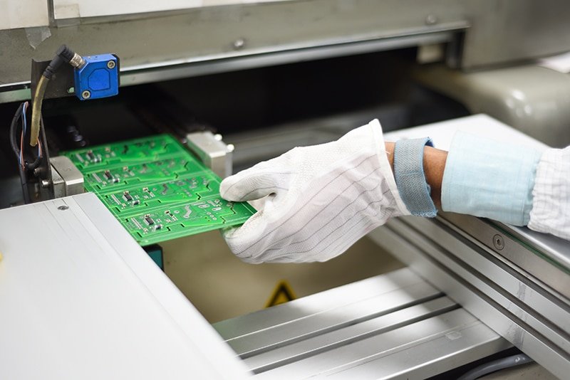
- Photoresist Removal: After etching, the remaining photoresist is stripped away, revealing the finished copper traces.
- Cleaning and Inspection: The board is thoroughly cleaned to remove any residual chemicals and inspected for defects or incomplete etching.

Types of Etching Techniques Used in PCB Manufacturing
There are several methods used to remove copper during the etching stage. The choice depends on factors such as production scale, board complexity, and environmental considerations.
- Wet Chemical Etching: The most common approach, using chemical solutions to dissolve unwanted copper. It is suitable for both prototype and mass production.
- Dry Etching (Plasma Etching): Utilizes plasma or ionized gases to remove copper. This method offers high precision but is more expensive and typically reserved for advanced applications.
- Mechanical Etching: Involves physically milling away copper using CNC machines. While less common, it is sometimes used for rapid prototyping or specialized designs.
Each technique has its own advantages and limitations, but wet chemical etching remains the industry standard due to its efficiency and scalability.
Materials and Chemicals Involved in the Etching Process
The PCB etching process explained in terms of materials highlights the importance of choosing the right chemicals and substrates. The most widely used etchants include:
- Ferric Chloride (FeCl3): Popular for its effectiveness and ease of handling, though it requires careful disposal due to environmental concerns.
- Ammonium Persulfate (NH4)2S2O8: Produces cleaner results and is less likely to stain, but is more expensive.
- Cupric Chloride (CuCl2): Can be regenerated and reused, making it more sustainable for large-scale production.
The choice of etchant depends on cost, safety, environmental regulations, and the specific requirements of the PCB design.
Best Practices for Accurate and Safe PCB Etching
Achieving high-quality results in PCB production requires attention to detail and adherence to safety protocols. Here are some essential tips:
- Work in a well-ventilated area: Many etchants release fumes that can be harmful if inhaled.
- Wear protective equipment: Gloves, goggles, and aprons protect against chemical splashes.
- Monitor etching progress: Over-etching can erode traces, while under-etching leaves unwanted copper.
- Dispose of chemicals responsibly: Follow local regulations for hazardous waste to minimize environmental impact.
- Inspect the board after etching: Use magnification to check for shorts, opens, or incomplete traces.
Common Challenges and How to Overcome Them
Even with careful preparation, issues can arise during the etching stage. Some of the most frequent challenges include:
- Under-etching: Occurs when copper is not fully removed, often due to expired or weak etchant. Solution: Use fresh chemicals and ensure proper agitation.
- Over-etching: Results in thin or broken traces. Solution: Monitor the process closely and remove the board as soon as etching is complete.
- Poor adhesion of photoresist: Can lead to pattern lifting or incomplete protection. Solution: Clean the copper surface thoroughly before applying photoresist.
- Environmental hazards: Mishandling of chemicals can cause pollution or health risks. Solution: Always follow recommended safety and disposal guidelines.
Many of these issues can be prevented by following established procedures and maintaining a clean, organized workspace.
Integrating Etching into the Full PCB Production Cycle
Etching is just one part of the broader electronics manufacturing process. After etching, boards typically undergo drilling, solder mask application, silkscreen printing, and component assembly. For a comprehensive overview of related topics, you might explore resources on electronics fabrication basics or learn about the difference between SMT and through hole assembly.
For further reading on the entire electronics manufacturing workflow, this complete process of electronic manufacturing services article provides an in-depth look at each stage, including how etching fits into the larger picture.
Frequently Asked Questions
What is the main purpose of etching in PCB production?
The primary goal of etching is to remove unwanted copper from the board, leaving behind the precise circuit pathways that connect electronic components. This step is essential for ensuring the board functions as intended.
Which chemicals are most commonly used for PCB etching?
The most widely used etchants include ferric chloride, ammonium persulfate, and cupric chloride. Each has its own advantages in terms of cost, effectiveness, and environmental impact.
How can I avoid over-etching or under-etching my PCB?
To achieve optimal results, monitor the etching process closely, use fresh chemicals, and remove the board as soon as the unwanted copper is dissolved. Proper agitation and temperature control also help ensure even etching.
Is PCB etching safe to do at home?
While it is possible to etch PCBs at home, it requires careful handling of chemicals, proper ventilation, and adherence to safety protocols. Always wear protective gear and dispose of chemicals responsibly.
Conclusion
Mastering the etching stage is fundamental for anyone involved in electronics design or manufacturing. By understanding the steps, materials, and best practices involved, you can produce reliable, high-quality circuit boards for a wide range of applications. Whether you’re a hobbyist or part of a professional production team, a solid grasp of this process will help you achieve better results and avoid common pitfalls.