

In today’s rapidly evolving electronics industry, ensuring the quality and reliability of Printed Circuit Boards (PCBs) is crucial. One method that has gained prominence for its precision and effectiveness is X ray inspection for PCBs. This technique not only identifies defects but also enhances the overall quality assurance process. Manufacturers, exporters, and importers alike are increasingly leaning towards this advanced method to meet industry standards.

What is X Ray Inspection?
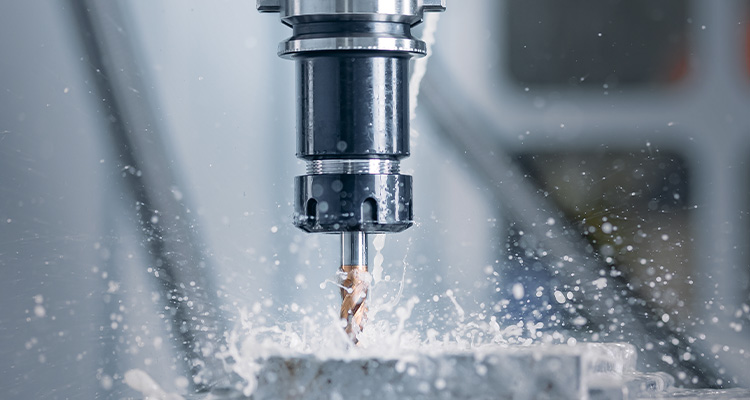
X ray inspection is a non-destructive testing method that uses X-rays to capture images of PCBs without causing any damage. By penetrating the layers of the board, it identifies defects such as voids, misalignments, and copper bridging that are not easily detectable by the naked eye.
Importance of X Ray Inspection in PCBs
The importance of X ray inspection for PCBs lies in its ability to ensure the integrity and functionality of electronic components. As electronic devices continue to become more intricate, the demand for flawless PCBs has skyrocketed. By utilizing this method, manufacturers can guarantee superior quality and minimize the risk of product failures.
Benefits of X Ray Inspection
Among the primary advantages of this method are:
- Non-destructive analysis.
- Enhanced fault detection capabilities.
- Ensures compliance with industry standards.
- Significantly reduces wastage and production costs.
How Does X Ray Inspection Work?
The process involves passing X-rays through the PCB while capturing detailed images. These images allow technicians to examine the internal structure of the board, identify defects, and assess the overall quality. This meticulous analysis helps in preventing future errors and ensuring product reliability.
Implementing X Ray Inspection in the Manufacturing Process
Integrating X ray inspection for PCBs into the manufacturing line ensures efficiency in quality control. This method can be easily incorporated into existing processes, allowing for seamless inspections.
Trends in PCB Inspection Technologies
As industries advance, the need for reliable and efficient inspection technologies grows. Current trends indicate an increasing reliance on X ray inspection due to its accuracy and ability to keep pace with technological innovations.
Challenges in PCB Inspection
Despite its advantages, challenges such as initial setup costs and the need for skilled technicians can be hurdles in adopting X ray inspection for PCBs. However, these can be mitigated with proper training and equipment sourcing.
The Role of Exporters and Importers
Exporters and importers play a significant role in ensuring that PCBs meet stringent quality standards. By leveraging X ray inspection, they can ensure compliance and enhance trust in the supply chain. This commitment to quality also opens new opportunities in global markets.
Case Studies: Successful Implementations
Several leading electronics manufacturers have successfully integrated X ray inspection for PCBs, leading to significant improvements in their quality control processes. These case studies underline the effectiveness and necessity of adopting such advanced inspection techniques.
Future Prospects of X Ray Inspection
The future of this technology is promising. As more industries recognize its value, the adoption of X ray inspection for PCBs is expected to grow, ensuring even higher standards of quality and reliability.
Related Resources
For those interested in further reading, exploring how technology impacts supply chains, understanding electronic prototypes, and exploring sustainable electronics will provide insightful information.

Frequently Asked Questions
How does X Ray inspection benefit PCB manufacturers?
X ray inspection provides a detailed analysis of internal structures, ensuring any defects are identified and rectified promptly, hence improving the overall product quality.
Is X Ray inspection safe for all types of PCBs?
Yes, it is safe for all PCBs as it is a non-destructive test. It does not cause any damage while inspecting the internal layers of the boards.
What challenges do companies face when implementing X Ray inspection?
The main challenges include initial setup costs and the need for trained professionals to interpret the detailed imagery accurately.
Where can I learn more about PCB manufacturing?
You can gain more insights by visiting blogs on custom electronics manufacturing.