

The development of wifi enabled electronic product design process has become a cornerstone for modern connected devices. From smart home appliances to industrial IoT solutions, integrating wireless connectivity is now a standard expectation. However, designing such products involves a series of complex steps that require careful planning, technical expertise, and a deep understanding of both electronics and wireless protocols.
This article provides a practical overview of how to approach the creation of electronics with built-in WiFi capabilities. Whether you are a startup founder, product manager, or an engineer, understanding the stages and best practices can help you avoid costly mistakes and accelerate time to market. For a more general overview of development stages, you may also find the electronic prototyping process guide helpful as a foundational resource.
Key Stages in Wireless Product Development
Building a device with WiFi functionality requires a structured approach. The process typically unfolds in several phases, each with distinct objectives and deliverables. Below, we outline the essential steps that guide teams from concept to production.
Requirements Gathering and Feasibility Analysis
Every successful project starts with a clear understanding of what the product needs to achieve. During this phase, teams define user requirements, connectivity needs, power constraints, and environmental considerations. It’s also crucial to assess the feasibility of integrating WiFi based on available chipsets, regulatory requirements, and cost targets.
- Identify user scenarios and connectivity expectations
- Evaluate existing solutions and technology stacks
- Estimate power consumption and battery life
- Consider certifications and compliance (e.g., FCC, CE)
System Architecture and Component Selection
With requirements in place, the next step is to design the system architecture. This involves selecting the right microcontroller or processor, WiFi module or SoC, antennas, and supporting components. The choice of WiFi standard (e.g., 802.11b/g/n/ac/ax) will impact performance, range, and compatibility.
It’s important to balance performance with power efficiency and cost. Many teams consult resources like the comprehensive guide to electronics design services and the design process to stay updated on best practices and component trends.

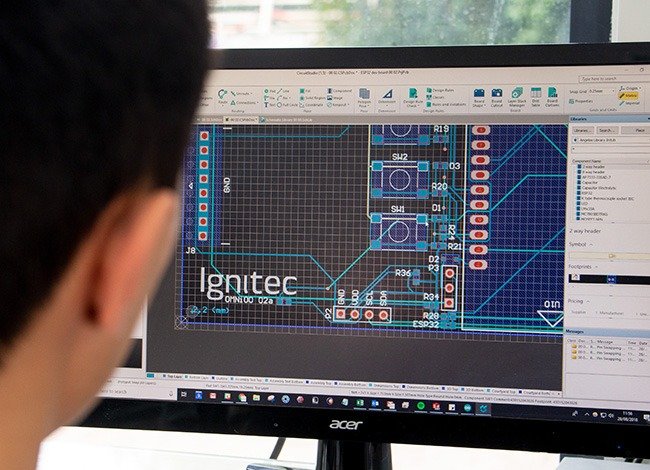
PCB Design and Prototyping for WiFi Devices
The printed circuit board (PCB) is the backbone of any electronic device. For products with wireless connectivity, careful PCB layout is critical to ensure signal integrity and minimize interference. The wifi enabled electronic product design process at this stage focuses on both electrical performance and manufacturability.
RF Considerations and Antenna Placement
One of the most challenging aspects of integrating WiFi is managing radio frequency (RF) performance. Antenna placement, ground planes, and shielding must be optimized to achieve reliable wireless communication. Simulation tools and iterative prototyping are often used to refine the design before moving to mass production.
- Use proper impedance matching for RF traces
- Minimize noise sources near the antenna
- Test different antenna types (chip, PCB, external)
- Validate wireless range and throughput in real environments
Rapid Prototyping and Functional Testing
Once the initial PCB is designed, rapid prototyping allows teams to assemble and test early hardware. This phase is essential for verifying core functionality, debugging firmware, and evaluating wireless performance. Issues discovered here can be addressed before committing to expensive tooling or certification.
For a more detailed breakdown of prototyping steps, refer to the electronic product design process steps article, which covers validation and iteration in greater depth.

Firmware Development and Connectivity Integration
The software layer is just as important as the hardware. Developing robust firmware ensures that the device can connect to WiFi networks, handle security protocols, and communicate with cloud services or mobile apps. This stage of the wifi enabled electronic product design process often involves:
- Implementing WiFi stack and network protocols (TCP/IP, MQTT, HTTP, etc.)
- Managing over-the-air (OTA) updates for future-proofing
- Optimizing power management for battery-operated devices
- Ensuring secure authentication and data encryption
Testing connectivity in various environments—such as different routers, signal strengths, and network configurations—is crucial to ensure a seamless user experience.
Certification, Compliance, and Mass Production
Before a WiFi-enabled product can be sold, it must comply with regional wireless regulations and safety standards. This typically involves third-party testing and certification (e.g., FCC in the US, CE in Europe). Failing to meet these requirements can result in costly delays or recalls.
After passing certification, the design is transferred to manufacturing. Production testing is implemented to ensure every unit meets quality and performance standards. Supply chain management and logistics planning also become critical at this stage.
Best Practices for Connected Device Design
To improve outcomes and reduce risks, consider these best practices throughout your project:
- Engage with experienced design partners early
- Document requirements and changes meticulously
- Iterate quickly with prototypes and user feedback
- Plan for scalability and future updates
- Stay informed on evolving wireless standards and security threats
For further insights into embedded solutions, the embedded systems product design services explained resource offers a deeper look at integrating connectivity and intelligence into products.
Frequently Asked Questions
What are the main challenges in designing WiFi-enabled electronics?
The biggest challenges include managing RF interference, optimizing antenna placement, ensuring regulatory compliance, and developing secure, reliable firmware. Each of these areas requires specialized knowledge and careful testing.
How long does it take to develop a connected device?
Timelines vary based on complexity, but a typical project can take anywhere from six months to over a year. Early planning, rapid prototyping, and clear requirements can help speed up the process.
Do I need to certify my product if it uses a pre-certified WiFi module?
Using a pre-certified module can simplify compliance, but final products may still require testing, especially if the antenna or layout changes. Always consult with certification experts to avoid surprises.
For a broader perspective on the advantages of professional design support, see the benefits of electronic product design services article.