

Printed circuit boards (PCBs) are the backbone of modern electronics, providing the physical platform for mounting and connecting electronic components. At the heart of every PCB are the traces—thin lines of conductive material that form the electrical pathways between components. Understanding why PCB traces matter is essential for anyone involved in electronics design, manufacturing, or quality control. These seemingly simple lines play a critical role in determining the performance, reliability, and manufacturability of electronic devices.
Whether you are designing a simple LED circuit or a complex multi-layer board for industrial equipment, the way you lay out your traces can make or break your project. In this article, we’ll explore the importance of trace design, how it impacts circuit behavior, and best practices to ensure optimal results. For those interested in the broader context of electronics manufacturing, you may also want to review electronics packaging types to see how PCB layout fits into the full product lifecycle.
The Role of PCB Traces in Electrical Performance
The primary function of PCB traces is to carry electrical signals and power between components. However, their influence goes far beyond simple connectivity. The width, length, and routing of traces directly affect resistance, capacitance, and inductance, which in turn impact signal integrity and power delivery.
- Signal Integrity: Poorly designed traces can cause signal degradation, crosstalk, or electromagnetic interference (EMI), especially in high-speed or high-frequency circuits.
- Power Distribution: Inadequate trace width can lead to voltage drops or overheating, risking component failure or reduced lifespan.
- Impedance Control: For RF and high-speed digital circuits, maintaining controlled impedance through trace geometry is essential for reliable operation.
These factors highlight why PCB traces matter so much in achieving both functional and reliable electronic designs.

How Trace Design Affects Manufacturing and Assembly
The layout of traces not only determines electrical performance but also influences the manufacturability of the PCB. Trace width, spacing, and routing complexity can affect yield rates, production costs, and inspection requirements.
- Minimum Trace Width and Spacing: PCB fabrication processes have limits on how thin traces can be and how close they can be placed. Violating these limits can result in open circuits or shorts.
- Thermal Management: Wider traces can help dissipate heat, which is especially important for power circuits or densely packed boards.
- Assembly Compatibility: Trace placement must consider component footprints and soldering processes to avoid assembly defects.
For a deeper dive into the steps involved in turning a schematic into a finished board, check out the electronics fabrication workflow guide.
Common Trace Design Mistakes and How to Avoid Them
Even experienced designers can make errors that compromise the effectiveness of their PCBs. Here are some frequent pitfalls and strategies to prevent them:
- Undersized Traces: Using traces that are too narrow for the expected current can cause excessive heating or even melting. Always calculate the required width based on current and copper thickness.
- Sharp Angles: Right-angle bends can create signal reflections and make etching more difficult. Use 45-degree angles or curved traces for smoother signal flow.
- Poor Grounding: Inadequate ground planes or fragmented ground traces can introduce noise and reduce EMC performance. Maintain continuous ground paths wherever possible.
- Overcrowding: Placing traces too close together increases the risk of shorts and complicates inspection. Respect the minimum spacing rules set by your PCB manufacturer.

Best Practices for Effective Trace Layout
To maximize the benefits of well-designed traces, consider the following recommendations:
- Use Adequate Trace Widths: Refer to IPC-2221 standards or manufacturer calculators to determine the right width for power and signal traces.
- Keep Traces Short and Direct: Shorter traces reduce resistance and inductance, improving signal quality and reducing EMI risk.
- Separate Analog and Digital Paths: Isolate sensitive analog traces from noisy digital lines to prevent interference.
- Implement Solid Ground Planes: A continuous ground plane beneath signal traces helps with noise suppression and impedance control.
- Follow Manufacturer Guidelines: Always consult your PCB fabricator’s capabilities for minimum trace width, spacing, and layer stackup.
Adhering to these principles ensures that your designs are robust, manufacturable, and reliable in real-world applications. For additional tips on producing high-quality assemblies, see the article on electronic assembly best practices.
Trace Design and Quality Control
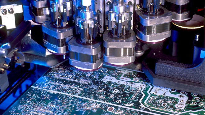
Quality assurance is a crucial aspect of electronics production, and trace layout plays a significant role in inspection and testing. Automated optical inspection (AOI) systems check for trace continuity, spacing violations, and potential defects before assembly proceeds. Well-designed traces simplify these checks and reduce the risk of costly rework.
For a comprehensive overview of inspection methods and standards, you can explore electronics quality control explained.
Learning More About PCB Trace Fundamentals
If you are new to PCB design or want to deepen your understanding, there are many resources available. One excellent starting point is the SparkFun PCB basics tutorial, which covers the essentials of board layout, trace routing, and more.
As technology advances and circuits become more complex, the importance of thoughtful trace design only increases. Whether you are working on prototypes or mass production, investing time in learning and applying best practices will pay dividends in product performance and reliability.
Frequently Asked Questions
What happens if PCB traces are too thin?
If traces are too narrow for the current they carry, they can overheat, leading to potential failure or even fire hazards. Thin traces also have higher resistance, which can cause voltage drops and affect circuit performance.
How do trace layouts affect signal integrity?
Trace geometry, length, and proximity to other signals influence capacitance, inductance, and crosstalk. Poor routing can cause signal reflections, noise, and data errors, especially in high-speed circuits.
What tools can help with PCB trace design?
Most PCB CAD software includes trace width calculators, design rule checks (DRC), and simulation tools to help optimize trace layout. Consulting manufacturer guidelines and industry standards is also recommended.