

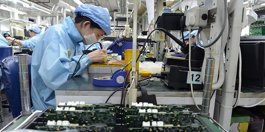
Printed circuit boards (PCBs) are the backbone of modern electronics, connecting and supporting electronic components in everything from smartphones to industrial machinery. During the manufacturing and assembly process, ensuring that each circuit functions as intended is crucial. This is where test points come into play. Understanding their purpose, design, and placement helps engineers, technicians, and manufacturers streamline testing, troubleshooting, and quality control.
In this article, we’ll explore the function and importance of these small but vital features found on PCBs. We’ll also discuss how they’re used in practice, their impact on assembly and maintenance, and offer practical insights for those involved in electronics design or production. For a deeper dive into related manufacturing processes, you might also be interested in learning how PCB drilling works and how it affects the placement of these critical contact points.
Understanding the Role of Test Points in PCB Design
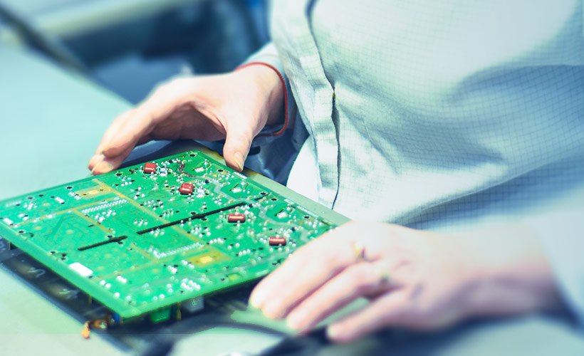
At their core, test points are designated locations on a PCB that provide convenient electrical access to specific nodes or traces within a circuit. These spots are intentionally exposed—often as small pads, vias, or pins—so that testing equipment or probes can make contact during manufacturing, assembly, or maintenance. The main objective is to verify electrical continuity, measure signals, or diagnose faults without damaging components or disrupting the circuit.
In the context of automated testing, these access points are essential for ensuring that each board meets the required specifications before it leaves the factory. They allow for rapid, repeatable measurements and help identify defects early in the production process.
Types of Test Points and Their Placement
There are several forms that these contact locations can take, each suited to different testing needs and manufacturing environments:
- Surface pads: Flat, exposed copper areas on the PCB surface, designed for easy probe contact.
- Through-hole vias: Plated holes that can be accessed from either side of the board, often used for double-sided probing.
- Pin headers: Rows of pins that allow for connection to test harnesses or fixtures.
- Looped wires: Small wire loops soldered to the board for manual probing or debugging.
Placement is a critical aspect of effective PCB testing. Designers must ensure that these points are accessible to probes or test fixtures, not obstructed by tall components, and spaced to prevent accidental shorts. The number and location of access points depend on the complexity of the circuit and the required test coverage.

Why Are Test Points Essential in Electronics Manufacturing?
Incorporating test points into a PCB layout brings several advantages throughout the product lifecycle:
- Efficient testing: Automated test equipment (ATE) can quickly connect to these locations, enabling high-speed, accurate verification of circuit functionality.
- Troubleshooting: When a board fails, technicians can use these access points to measure voltages, signals, or continuity, speeding up diagnosis and repair.
- Quality assurance: Consistent and repeatable testing helps maintain high manufacturing standards and reduces the risk of defective products reaching customers.
- Maintenance: For products requiring field service, these locations simplify ongoing diagnostics and repairs.
The importance of these features is especially apparent in high-volume manufacturing, where rapid, automated testing is essential to keep production lines moving efficiently. For a comprehensive overview of the electronics production workflow, see this complete guide to electronic manufacturing services.
Design Considerations for Effective Test Point Implementation
Integrating these access locations into a PCB requires balancing testability with other design constraints. Here are some best practices to consider:
- Accessibility: Ensure that probes or test fixtures can reach the points without interference from components or board edges.
- Spacing: Maintain adequate distance between points to prevent accidental shorts and allow for reliable probe contact.
- Pad size: Use sufficiently large pads to accommodate the type of probe or fixture used in testing.
- Signal integrity: Avoid placing access points on high-speed or sensitive traces where added capacitance or inductance could affect performance.
- Marking: Clearly label each point on the silkscreen layer to aid technicians during manual testing or debugging.
In some cases, designers may need to compromise between maximizing test coverage and minimizing board size or cost. Early collaboration between design, test, and manufacturing teams helps ensure that these features are both effective and practical.
How Test Points Support Automated and Manual Testing
Both automated and manual testing rely on these designated locations for efficient circuit verification. In automated environments, test fixtures equipped with spring-loaded pins (often called “pogo pins”) make simultaneous contact with multiple points, allowing for rapid, parallel measurements. This approach is common in large-scale manufacturing, where throughput and consistency are paramount.
For manual testing, technicians use handheld probes or multimeters to access these points individually. This is especially useful during prototyping, debugging, or field service, where flexibility and direct measurement are needed.
The presence of well-placed access points can dramatically reduce testing time, minimize the risk of damaging components, and improve the reliability of both automated and manual verification processes.
Common Challenges and Solutions in Test Point Design
Despite their benefits, integrating these features into a PCB is not without challenges. Some common issues include:
- Limited board space: High-density designs may leave little room for additional pads or vias.
- Component interference: Tall or closely packed components can obstruct probe access.
- Signal interference: Poor placement can introduce noise or affect sensitive signals.
Solutions often involve careful planning during the layout phase, such as grouping access points along the board edge, using smaller pads, or leveraging unused vias. In some cases, designers may employ multiplexed testing, where a single point is used to access multiple signals through switching circuits.
Frequently Asked Questions
What is the main purpose of test points on a circuit board?
Their primary function is to provide convenient, non-destructive access to specific nodes within a circuit for electrical testing, troubleshooting, and quality control. They help verify that the board operates as intended before it is shipped or deployed.
How do you choose the right locations for test points?
Placement should prioritize accessibility for probes or fixtures, avoid interference with components, and ensure adequate spacing to prevent shorts. Designers often select locations that represent critical signals, power rails, or ground connections for comprehensive testing.
Can test points affect the performance of a PCB?
If not carefully designed, these features can introduce unwanted capacitance or inductance, especially on high-speed or sensitive traces. To minimize impact, use the smallest practical pad size, avoid critical signal paths, and consult with signal integrity experts during layout.
Are test points necessary for all PCB designs?
While not mandatory for every board, they are highly recommended for complex or high-volume products where thorough testing and troubleshooting are essential. Simpler designs or one-off prototypes may use fewer or no dedicated access points, depending on testing requirements.
Conclusion
Integrating test points into PCB layouts is a best practice that enhances testing efficiency, improves quality assurance, and simplifies troubleshooting throughout the product lifecycle. By understanding their role, types, and design considerations, engineers and manufacturers can ensure more reliable and maintainable electronic products. For further reading on related topics, you may also find value in exploring what is impedance control in PCBs and other electronics fabrication safety tips.