

Understanding how to interpret PCB (Printed Circuit Board) schematics is a fundamental skill for anyone interested in electronics. This guide aims to help beginners navigate the complex world of PCB diagrams.
Before we dive into the specifics, it’s worth noting the importance of hardware design documentation. It’s a critical aspect of any hardware design process, including PCB design.
Basics of PCB Schematics
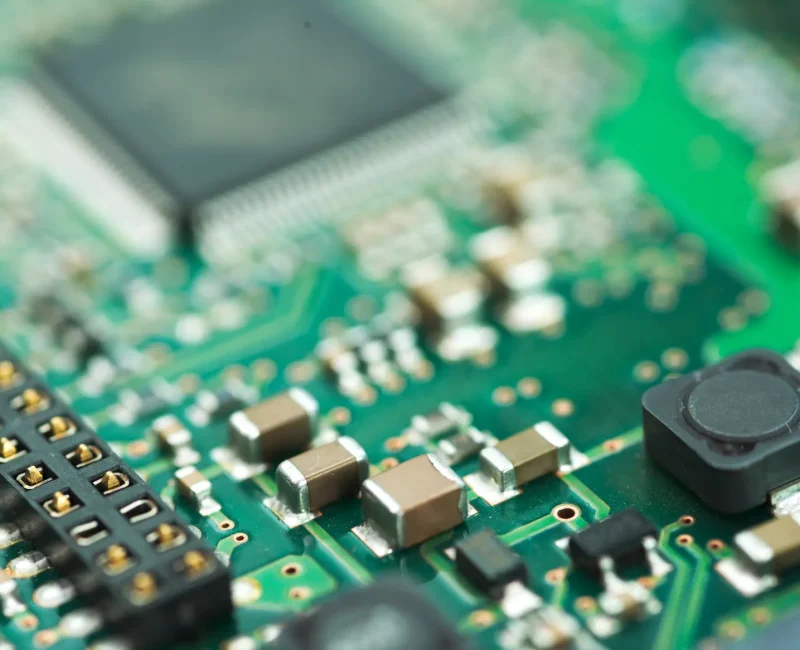
PCB schematics are visual representations of circuits and their components. They consist of symbols that represent different components, lines that depict connections, and labels that provide additional information.
Understanding Symbols and Connections
Each symbol in a PCB schematic represents a specific component, such as resistors, capacitors, or transistors. Lines between these symbols illustrate the connections between components, forming the circuit.
Reading Labels and Annotations
Labels and annotations provide additional details about components and connections. They might include information about component values, part numbers, or connection types.

Practical Tips for Reading PCB Schematics
As a beginner, it can be helpful to start by identifying the main components and tracing the connections between them. Practice is key – the more schematics you read, the more comfortable you’ll become with the symbols and conventions.
For more insights into the world of hardware design, check out this article on rapid prototyping solutions for hardware innovation.
By Ethan Carter, published on October 28, 2025