

Creating a printed circuit board (PCB) from the ground up is a fundamental skill for electronics engineers, hobbyists, and product designers. Whether you’re developing a prototype or planning for mass production, understanding how to design a PCB efficiently can save time, reduce costs, and improve product reliability. This guide walks you through the essential steps, from initial concept to a ready-to-manufacture design, highlighting best practices and common pitfalls to avoid.
Before diving into the technical process, it’s important to grasp the role of PCBs in modern electronics. These boards provide the physical platform for mounting and interconnecting electronic components, ensuring electrical connectivity and mechanical support. As you progress through the design stages, you’ll encounter decisions that impact manufacturability, performance, and cost.
If you’re new to the field, it’s helpful to understand what is a gerber file, as these files are essential for PCB fabrication and assembly.
Planning Your PCB Project
Every successful board starts with careful planning. Begin by defining your project’s requirements, including the intended function, size constraints, and environmental considerations. List all necessary components and determine the type of board—single-sided, double-sided, or multi-layered—based on circuit complexity and performance needs. For more insight into board construction, see this overview of understanding PCB layers.
- Schematic design: Draw a circuit diagram using electronic design automation (EDA) software. This schematic is the blueprint for your layout.
- Component selection: Choose reliable, readily available parts. Consider package types, voltage ratings, and power requirements.
- Board outline: Define the physical dimensions and shape early to avoid costly redesigns later.
Translating Schematics to PCB Layout
Once your schematic is complete, the next step is transferring it to a physical layout. This process involves placing components and routing electrical connections on the board. Modern EDA tools simplify this task, but attention to detail is crucial for signal integrity and manufacturability.

Component Placement Strategies
Good component placement is foundational to a reliable PCB. Place critical parts such as microcontrollers, connectors, and power supplies first. Group related components to minimize trace lengths and reduce electromagnetic interference. Leave adequate space for heat dissipation and consider mechanical constraints like mounting holes.
Routing and Layer Management
Routing refers to drawing the copper traces that connect components. For simple circuits, single or double-sided boards may suffice. More complex designs may require multiple layers to separate power, ground, and signal paths. If you’re unsure about the differences, explore the difference between SMT and through hole assembly to select the right technology for your project.
- Signal traces: Keep traces as short and direct as possible to reduce noise and signal loss.
- Power and ground planes: Use dedicated layers for power and ground to improve stability and reduce interference.
- Clearances: Follow manufacturer guidelines for minimum trace width and spacing to ensure manufacturability and safety.
Design Rules and Verification
Adhering to design rules is essential for a functional and manufacturable board. Most EDA tools allow you to set constraints for trace width, spacing, via sizes, and more. Running a design rule check (DRC) helps catch errors before production.
Additionally, perform an electrical rule check (ERC) to verify that all connections are correct and that there are no unintentional shorts or opens. Simulate your circuit if possible to identify potential issues with signal integrity or power distribution.
Preparing Manufacturing Files
After finalizing your layout, generate the necessary files for fabrication. The most common format is the Gerber file, which contains all the information a manufacturer needs to produce your board. Double-check all layers, including silkscreen, solder mask, and drill files, to ensure accuracy.
For a detailed explanation of the manufacturing process, you can refer to this resource on electronics manufacturing steps.
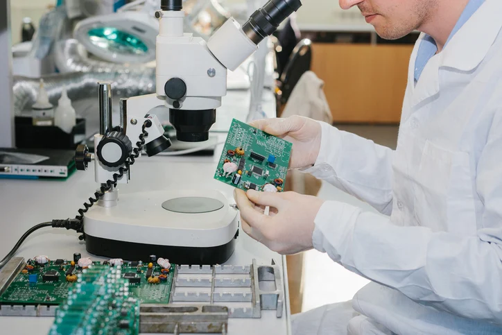
Prototyping and Testing Your Board
Before committing to a full production run, it’s wise to build a prototype. This allows you to test the board’s functionality, identify design flaws, and make necessary adjustments. Use a reputable assembly service or assemble the board yourself if you have the skills and equipment.

- Visual inspection: Check for solder bridges, missing components, and correct orientation.
- Continuity testing: Use a multimeter to verify that all connections are as intended.
- Functional testing: Power up the board and test its performance under real-world conditions.
For advanced testing methods and standards, consider reviewing this guide to electronic component testing techniques.
Optimizing Your PCB Design for Production
Once your prototype is validated, you may need to optimize your design for large-scale manufacturing. This can involve panelization (grouping multiple boards for efficient fabrication), refining component footprints, and ensuring compliance with industry standards. Work closely with your manufacturer to address any concerns about materials, tolerances, or assembly processes.
It’s also important to consider the assembly method. Surface-mount technology (SMT) is common for compact, high-volume products, while through-hole assembly may be better for robust or easily serviceable designs. Learn more about how SMT assembly works to make informed decisions.
Frequently Asked Questions
What software is recommended for PCB design?
Popular EDA tools include Altium Designer, Eagle, KiCad, and OrCAD. The best choice depends on your budget, project complexity, and personal preference. Open-source options like KiCad are suitable for beginners and small projects.
How can I avoid common mistakes when creating a PCB?
Double-check your schematic before starting the layout, adhere to manufacturer design rules, and always run design rule checks. Prototyping and thorough testing can help catch errors early. Consulting with experienced designers or manufacturers can also prevent costly oversights.
What files do manufacturers need to produce a PCB?
Manufacturers typically require Gerber files for each layer, a drill file for holes, and a bill of materials (BOM). Some may also request assembly drawings and pick-and-place files for automated assembly.
How do I select between single-layer and multi-layer PCBs?
Single-layer boards are suitable for simple circuits with few components. Multi-layer boards are necessary for complex designs that require more routing space, better signal integrity, or advanced power distribution.
Mastering the process of how to design a PCB opens the door to creating reliable, high-performance electronic products. By following structured steps, leveraging the right tools, and collaborating with manufacturers, you can turn your ideas into functional hardware ready for the real world.