

Printed circuit boards (PCBs) are at the heart of modern electronics, and one of their most critical protective features is the solder mask. This thin polymer layer shields copper traces from oxidation, prevents solder bridges during assembly, and ensures the reliability of electronic devices. Understanding how solder masks are made offers valuable insight into the manufacturing process and the quality standards behind reliable PCBs.
The journey from raw materials to a finished solder mask involves several precise steps, each contributing to the board’s durability and performance. Whether you are involved in electronics manufacturing, PCB design, or simply curious about the technology inside your devices, this guide will walk you through the essential stages of solder mask production.
For those interested in related topics, you may also want to explore electronics fabrication challenges to understand the broader context of PCB manufacturing.
The Role of Solder Masks in PCB Manufacturing
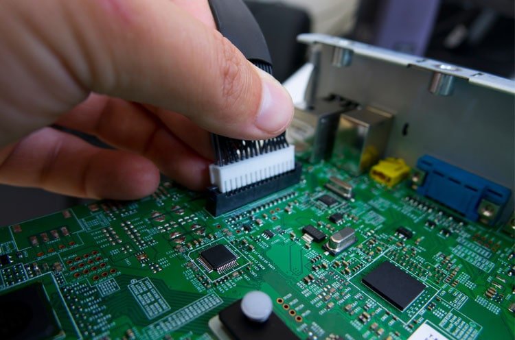
Before diving into the production process, it’s important to understand what a solder mask does. This protective coating is typically green but can come in other colors. It covers the non-conductive areas of a PCB, leaving only the pads and vias exposed for soldering. The mask prevents accidental solder bridges, reduces the risk of corrosion, and enhances the board’s electrical insulation.
In high-density designs, the precision of the solder mask application is crucial for avoiding short circuits and ensuring long-term reliability. This is especially relevant in advanced electronics where thermal management in electronics and miniaturization are key considerations.
Materials Used in Solder Mask Production
The main component of a solder mask is a liquid photoimageable (LPI) polymer, which is sensitive to ultraviolet (UV) light. These polymers are chosen for their excellent adhesion, chemical resistance, and ability to withstand high temperatures during soldering. Other types include epoxy liquid and dry film solder masks, but LPI is the most common in modern PCB fabrication.
- LPI Solder Mask: Offers high resolution and is suitable for fine-pitch designs.
- Epoxy Liquid: Applied by silkscreening, more common in less complex boards.
- Dry Film: Laminated onto the board, used for specific applications.
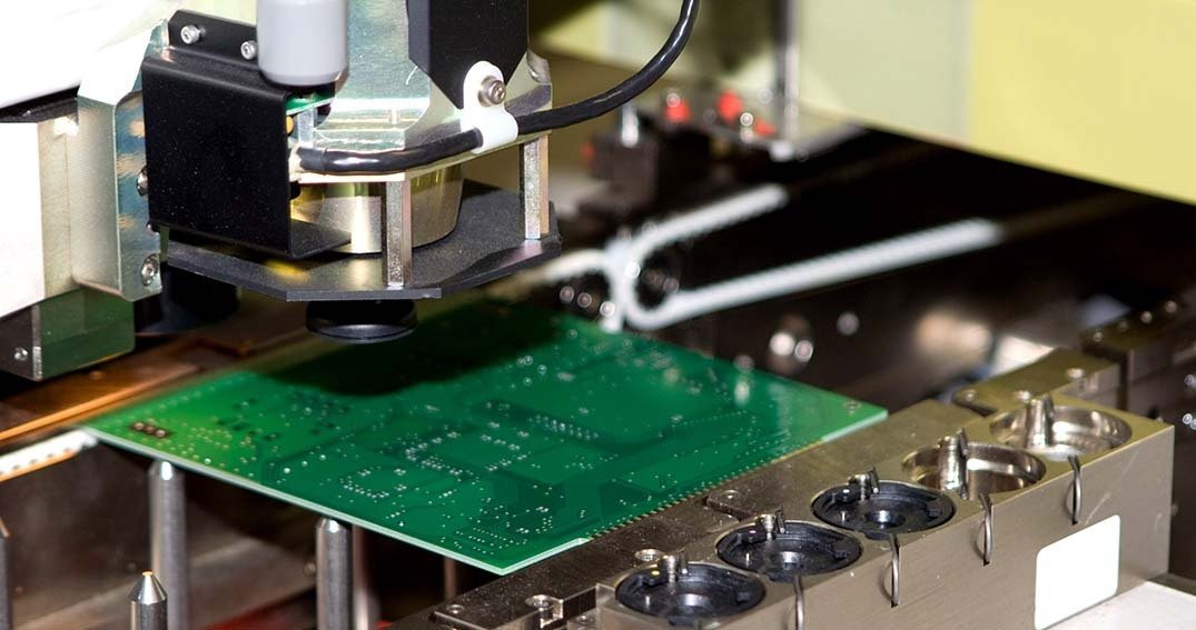
Step-by-Step Process: From Application to Curing
The process of how solder masks are made involves several carefully controlled stages. Each step ensures that the mask adheres properly, aligns with the circuit pattern, and provides robust protection.
1. Surface Preparation
The PCB surface must be meticulously cleaned to remove dust, oils, and oxidation. This is typically done using chemical cleaning agents and mechanical brushing. A clean surface is essential for the solder mask to bond effectively.
2. Solder Mask Application
The most common method is to coat the board with LPI solder mask. This can be done through:
- Spray Coating: The mask is sprayed evenly across the board, suitable for high-volume production.
- Curtain Coating: The board passes through a curtain of liquid mask, ensuring uniform thickness.
- Screen Printing: Used for epoxy liquid masks, suitable for simpler designs.
The thickness of the applied mask is controlled to ensure adequate coverage without interfering with component placement.
3. Pre-Drying
After application, the coated boards are partially dried (also called “tack drying”) in an oven. This step solidifies the mask enough to handle subsequent processing without smudging or deformation.
4. Image Development
The next stage involves aligning a photomask (a transparent film with the circuit pattern) over the board. The assembly is exposed to UV light, which hardens the solder mask in the exposed areas. The unexposed regions remain soft.
This photoimaging technique allows for precise definition of solder mask openings, which is critical for high-density and fine-pitch PCBs.
5. Developing and Rinsing
The board is then washed with a developer solution that removes the unhardened solder mask, revealing the copper pads and vias. Only the areas exposed to UV light remain protected.
6. Final Curing
The last step is a full thermal cure, where the board is baked at a specified temperature. This hardens the mask completely, ensuring strong adhesion and chemical resistance.
Quality Control and Inspection
After curing, the solder mask undergoes rigorous inspection. Automated optical inspection (AOI) systems check for defects such as pinholes, misalignment, or incomplete coverage. Any issues can compromise the board’s performance and reliability.
In addition to visual checks, some manufacturers perform electrical tests to ensure that the mask does not interfere with circuit continuity. For more on this aspect, see circuit continuity testing.
Common Challenges in Solder Mask Manufacturing
Producing a flawless solder mask is not without its difficulties. Some of the most common challenges include:
- Adhesion Issues: Poor cleaning or incompatible materials can lead to delamination.
- Registration Errors: Misalignment between the photomask and PCB can cause defects.
- Thickness Variations: Inconsistent application can result in weak protection or interference with assembly.
- Pinhole Defects: Tiny holes in the mask can expose copper, leading to corrosion or short circuits.
Addressing these challenges requires strict process control, regular equipment maintenance, and skilled operators. For a broader look at the hurdles faced in electronics production, refer to the article on electronics fabrication challenges.
Applications and Advancements in Solder Mask Technology
As electronics continue to evolve, so do the requirements for solder mask materials and processes. Modern trends include:
- High-Resolution Masks: Essential for fine-pitch and high-density interconnect (HDI) PCBs.
- Color Variations: Beyond green, colors like blue, black, and white are used for specific applications or branding.
- Improved Thermal Resistance: To withstand lead-free soldering and reflow processes.
- Environmentally Friendly Materials: Reducing volatile organic compounds (VOCs) and hazardous substances.
These advancements help manufacturers meet the growing demands of industries such as automotive, medical devices, and consumer electronics.
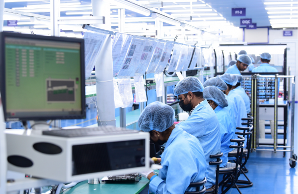
Manual Assembly and Solder Mask Considerations
When assembling PCBs by hand, the quality and accuracy of the solder mask can significantly impact the ease of soldering and the risk of defects. For those new to electronics assembly, this beginner’s guide to manual assembly provides practical tips for working with solder-masked boards.
Frequently Asked Questions
What is the main purpose of a solder mask on a PCB?
The solder mask acts as a protective layer that prevents solder bridges, shields copper traces from oxidation, and improves the electrical insulation of the board. It also enhances the board’s appearance and durability.
Can solder masks be repaired if damaged?
Minor defects in the solder mask can sometimes be repaired using specialized touch-up materials. However, significant damage may require reapplication or, in severe cases, remanufacturing of the PCB.
Are there different types of solder masks for various applications?
Yes, there are several types, including liquid photoimageable (LPI), epoxy liquid, and dry film solder masks. The choice depends on the complexity of the design, required resolution, and production volume.
How does solder mask thickness affect PCB performance?
Proper thickness ensures adequate protection without interfering with component placement. Too thin a layer may not provide sufficient insulation, while too thick can cause assembly issues.
Conclusion
The process of creating a solder mask is a blend of chemistry, precision engineering, and quality control. Each stage—from material selection to final inspection—plays a vital role in ensuring that PCBs function reliably in demanding environments. As technology advances, so too will the methods and materials used in this essential aspect of electronics manufacturing.
For those interested in learning more about related topics, you might also find value in reading about circuit design rules explained and how to use a multimeter for electronics testing.