


In the world of modern electronics manufacturing, pick-and-place machines are essential for assembling printed circuit boards (PCBs) quickly and accurately. These automated systems are responsible for placing tiny electronic components onto PCBs, a process that would be nearly impossible to achieve at scale by hand. Understanding how pick and place machines work can help engineers, hobbyists, and manufacturers appreciate the technology that powers today’s electronic devices.
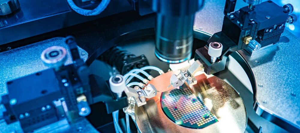
Before diving into the mechanics and workflow of these machines, it’s helpful to see how they fit into the broader context of electronics production. For a deeper look at the origins of the components themselves, you might find this guide on how electronics components are made useful.
The Role of Automated Placement in PCB Assembly
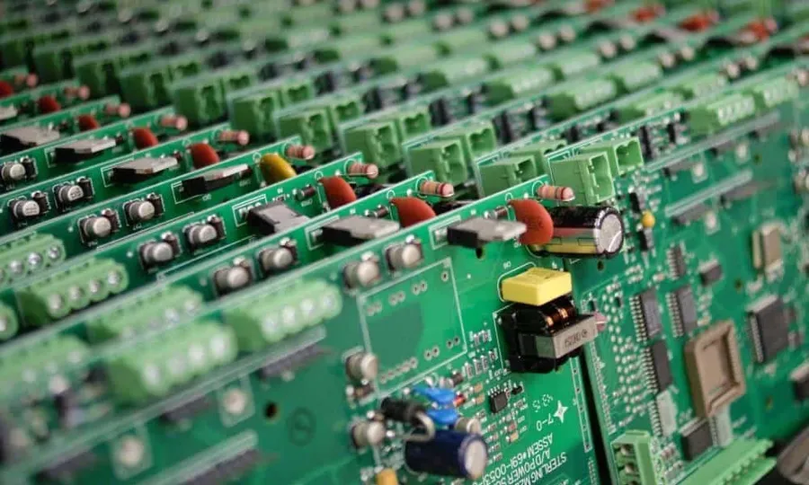
Automated placement equipment has revolutionized the assembly of electronic circuits. In traditional assembly, workers would manually position resistors, capacitors, and integrated circuits onto boards—a process that was slow and prone to errors. Today, pick and place machines handle this task with speed and precision, enabling mass production of everything from smartphones to industrial controllers.
These machines are a core part of surface-mount technology (SMT) lines. They take components supplied in reels, tubes, or trays and place them onto solder-pasted PCBs, ready for soldering. The result is a dramatic increase in throughput and consistency, which is crucial for high-volume manufacturing.
Key Components of Pick-and-Place Equipment
To understand how pick and place machines work, it’s helpful to break down their main parts:
- Feeders: These hold and supply the electronic components, usually in tape-and-reel, tube, or tray form. The feeder presents each part to the machine’s head for pickup.
- Placement Head: This is the “arm” of the machine, equipped with suction nozzles or grippers. It picks up components from the feeders and moves them to the correct location on the PCB.
- Vision System: Cameras and sensors guide the placement head, ensuring each part is picked and positioned accurately. The vision system can also inspect components for orientation and defects.
- Conveyor or Work Table: The PCB is transported into position for assembly, either by a conveyor belt or a stationary work table.
- Control Software: This software coordinates the entire process, translating PCB design files into precise movements and actions for the machine.
Step-by-Step: The Placement Process Explained
The operation of a pick-and-place machine follows a carefully orchestrated sequence:
- Loading the PCB: The bare board, already coated with solder paste, enters the machine via a conveyor.
- Component Pickup: The placement head moves to the feeder, where it uses a vacuum nozzle to pick up a component.
- Alignment and Inspection: The vision system checks the component’s orientation and position, making any necessary adjustments.
- Placement: The head moves to the designated spot on the PCB and places the component onto the solder paste.
- Repeat: This process is repeated for every component, often at speeds of thousands of placements per hour.
- Board Exit: Once all parts are placed, the PCB moves out of the machine, ready for the next step—typically reflow soldering.
Precision and Speed: What Makes These Machines So Effective?
The combination of high-speed movement and microscopic accuracy is what sets automated placement apart. Modern machines can place components as small as 01005 packages (just 0.4mm x 0.2mm) with placement rates exceeding 100,000 parts per hour in top-tier models. This level of performance is achieved through:
- Advanced motion control systems that synchronize the head and conveyor.
- Real-time vision correction to compensate for slight misalignments or board warping.
- Multiple nozzles on a single head, allowing simultaneous pickup and placement of several components.
- Optimized software algorithms that plan the most efficient sequence for each job.
For those interested in what happens after placement, such as soldering, you can explore related processes like how wave soldering works in PCB assembly.
Quality Assurance and Testing in Automated Assembly
Even with advanced automation, quality control remains critical. Most pick-and-place systems incorporate in-line inspection to catch errors early. After assembly, PCBs undergo further testing to ensure functionality. For a deeper dive into industry practices, you can read about electronic component testing standards and advanced techniques used to verify board quality.
Additional methods, such as automated optical inspection (AOI) and in-circuit testing, help manufacturers maintain high reliability in finished products. For more on this topic, see this overview of electronics testing methods.
Applications and Benefits of Automated Placement
The use of pick-and-place machines is widespread across industries. They are essential in the production of consumer electronics, automotive modules, medical devices, and industrial controls. The main benefits include:
- Increased throughput: Machines can assemble thousands of boards per day, far outpacing manual labor.
- Improved accuracy: Consistent placement reduces defects and rework.
- Flexibility: Modern systems can handle a wide range of component sizes and board layouts.
- Cost savings: Automation lowers labor costs and minimizes waste from errors.
If you’re interested in building your own PCBs or learning about materials used in prototyping, check out this DIY PCB fabrication guide and a list of essential circuit prototyping materials.
Frequently Asked Questions
What types of components can pick-and-place machines handle?
These machines are designed to work with a wide variety of surface-mount devices (SMDs), including resistors, capacitors, diodes, transistors, integrated circuits, and even some mechanical parts like connectors. Advanced models can also handle odd-shaped or delicate components with specialized nozzles and grippers.
How accurate are automated placement systems?
Modern pick-and-place equipment can achieve placement accuracy within a few microns, depending on the machine and component size. Vision systems and real-time correction algorithms ensure that even the smallest parts are positioned precisely on the PCB.
What happens after components are placed on the PCB?
Once all components are in position, the board typically moves to a reflow oven, where the solder paste melts and forms permanent electrical connections. Additional inspection and testing steps follow to verify the integrity and functionality of the assembled board.