

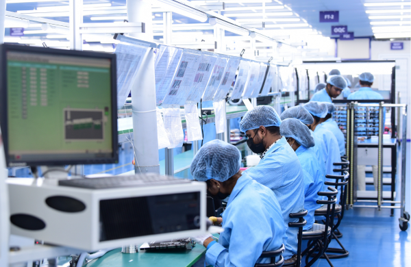
Printed circuit boards (PCBs) are the backbone of modern electronics, providing the essential pathways for electrical signals between components. One of the most critical steps in PCB manufacturing is the drilling process, which creates precise holes for mounting components and forming electrical connections between layers. Understanding how PCB drilling works is essential for engineers, designers, and anyone involved in electronics production, as it directly impacts the reliability and performance of the final product.
The drilling stage is far more than simply making holes. It requires advanced machinery, careful planning, and strict quality control to ensure each hole is positioned and sized correctly. In this guide, we’ll break down the methods, equipment, and best practices that define modern PCB drilling, helping you gain a clear picture of this vital fabrication step.
For those interested in optimizing every stage of circuit board production, it’s also important to consider factors like how to choose PCB substrate materials, as these choices can affect drilling techniques and outcomes.
Why Drilling Is Essential in PCB Fabrication
The creation of holes in a PCB serves several critical functions. Most obviously, these holes allow for the insertion of through-hole electronic components, such as resistors, capacitors, and connectors. Beyond that, drilled holes—also known as vias—enable electrical connections between different layers in multi-layer boards. Without precise drilling, these connections would be unreliable, leading to circuit failures or degraded performance.
The accuracy and cleanliness of each hole are vital. Even minor deviations can cause issues such as poor solder joints, misaligned components, or short circuits. As PCBs become more complex and miniaturized, the demands on drilling precision continue to increase.
Core Methods Used in PCB Drilling
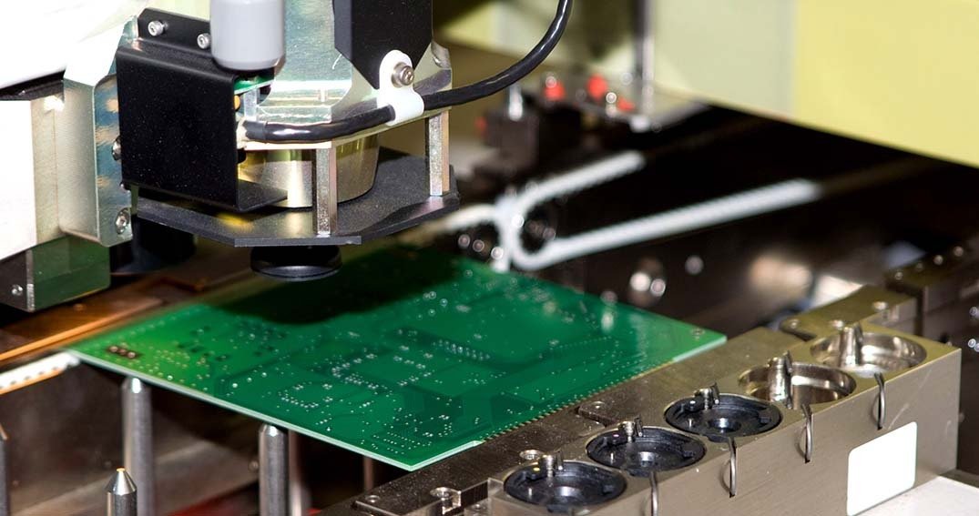
There are two main technologies used to create holes in PCBs: mechanical drilling and laser drilling. Each method has its own strengths and is chosen based on the board’s design, the required hole size, and production volume.
- Mechanical Drilling: This is the most common approach, using high-speed spindles equipped with tungsten carbide drill bits. Mechanical drills are capable of producing thousands of holes per hour with diameters typically ranging from 0.15 mm to several millimeters.
- Laser Drilling: For microvias and extremely small holes, lasers are used. This method is ideal for high-density interconnect (HDI) boards where space is at a premium. Laser drilling offers exceptional precision and is often used for holes less than 0.15 mm in diameter.
Step-by-Step Overview: The PCB Drilling Process
To fully understand how PCB drilling works, it’s helpful to look at the process step by step. Each phase is carefully controlled to ensure the highest quality and repeatability.
- Design and Preparation: The process begins with the PCB design, where the locations, sizes, and types of holes are specified in the Gerber files. These files are loaded into the drilling machine’s software.
- Stacking and Fixing: Multiple PCB panels may be stacked together to improve efficiency. The stack is secured to prevent movement during drilling.
- Drilling Execution: The drilling machine, guided by the design files, uses either mechanical bits or lasers to create the required holes. The machine’s accuracy is typically within a few microns.
- Deburring and Cleaning: After drilling, the holes may have small burrs or debris. These are removed through brushing, chemical cleaning, or plasma treatment to ensure smooth, clean holes.
- Inspection and Quality Control: Automated optical inspection (AOI) and manual checks confirm that all holes are present, correctly sized, and free from defects.
Types of Holes Created During Drilling
Not all holes on a PCB serve the same purpose. Understanding the different types helps clarify why specific drilling techniques are chosen:
- Through-Holes: These extend from the top to the bottom of the board, allowing for component leads or interlayer connections.
- Blind Vias: Connecting an outer layer to one or more inner layers without passing through the entire board.
- Buried Vias: These connect only internal layers and are not visible from the outside.
- Microvias: Extremely small vias, often created by laser drilling, used in HDI PCBs for dense component layouts.
Key Factors Affecting Drilling Quality
The effectiveness of the drilling process depends on several variables:
- Drill Bit Quality: Worn or low-quality bits can cause rough holes, excessive burrs, or even board damage.
- Machine Calibration: Regular calibration ensures that holes are positioned accurately according to the design.
- Material Selection: The choice of substrate affects drill wear and the risk of delamination. For more on this, see our guide on how to choose PCB substrate.
- Speed and Feed Rates: Optimizing the speed of drilling and the rate at which the bit advances prevents overheating and ensures clean cuts.
- Debris Removal: Effective evacuation of dust and chips keeps holes clean and prevents defects.
Modern Equipment and Automation in PCB Drilling
Advances in automation have transformed the way holes are created in circuit boards. Today’s CNC (computer numerical control) drilling machines can operate at extremely high speeds, with automatic tool changers and real-time monitoring systems. These machines can switch between different drill sizes and even between mechanical and laser drilling, depending on the design requirements.
Automation not only increases throughput but also reduces the risk of human error. With sophisticated software, manufacturers can simulate the drilling process before production, identifying potential issues and optimizing tool paths for efficiency and accuracy.
Common Challenges and How to Address Them
Even with advanced equipment, several challenges can arise during the drilling stage:
- Drill Bit Breakage: This can occur due to excessive wear, improper feed rates, or hard inclusions in the board material. Regular maintenance and monitoring help minimize this risk.
- Hole Wall Roughness: Caused by dull bits or incorrect speeds, rough hole walls can lead to poor plating and unreliable connections.
- Misregistration: If the holes are not aligned with the PCB pads, component mounting and electrical performance suffer. Accurate machine setup and regular calibration are essential.
- Delamination: Excessive heat during drilling can cause the layers of the PCB to separate. Using sharp tools and optimized drilling parameters helps prevent this.
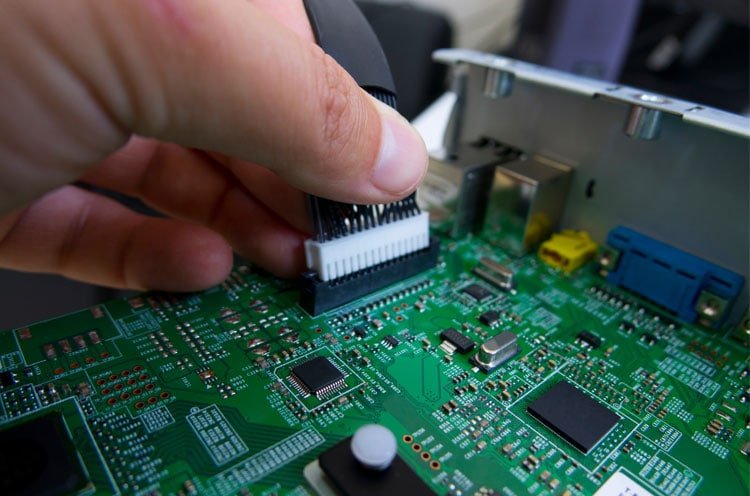
For those assembling boards by hand, understanding the importance of clean, accurate holes is just as crucial. Beginners can benefit from resources like this beginner’s guide to electronics projects and manual assembly, which covers practical tips for working with drilled PCBs.
Best Practices for Reliable PCB Drilling
To achieve the best results, manufacturers and designers should follow these best practices:
- Always use high-quality, sharp drill bits and replace them regularly.
- Ensure all drilling equipment is properly calibrated and maintained.
- Choose substrate materials that are compatible with the intended drilling method.
- Optimize drilling parameters (speed, feed rate) based on the board material and hole size.
- Implement thorough cleaning and inspection steps after drilling to remove debris and verify hole quality.
By following these guidelines, you can minimize defects, improve assembly yields, and ensure the long-term reliability of your electronic products.
Frequently Asked Questions
What is the smallest hole size achievable with current PCB drilling technology?
With mechanical drilling, the smallest practical hole size is typically around 0.15 mm. Laser drilling can achieve even smaller holes, down to 0.075 mm or less, making it suitable for high-density designs and microvias.
How does substrate material affect the drilling process?
The type of substrate impacts drill wear, heat generation, and the risk of delamination. Harder materials require tougher drill bits and slower feed rates, while softer materials may produce more debris. Selecting the right substrate is crucial for both drilling quality and overall board performance.
Why is hole cleanliness important in PCB manufacturing?
Clean holes are essential for reliable plating and electrical connections. Debris or roughness inside the holes can prevent proper metal deposition, leading to weak joints or open circuits. Thorough cleaning and inspection after drilling help ensure consistent quality.