

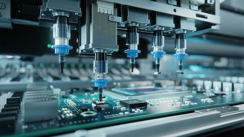
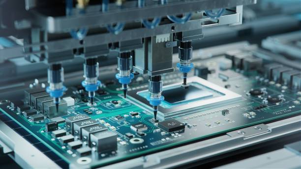
Managing heat within electronic circuits is a fundamental aspect of reliable device design. As components become smaller and more powerful, the challenge of dissipating excess heat grows. Electronics thermal relief refers to specific design strategies and features used to control and limit heat buildup in printed circuit boards (PCBs) and assemblies. Without proper attention to this topic, soldering quality, component lifespan, and overall device performance can suffer.
In this article, we’ll break down the concept of thermal relief in electronics, why it matters for both manufacturing and long-term reliability, and how it’s implemented in real-world designs. You’ll also find practical tips for engineers, hobbyists, and anyone interested in understanding the science behind keeping electronics cool and functional.
For a broader look at how heat is managed across different devices and applications, you may also want to explore our guide on thermal management in electronics.
Understanding Thermal Relief in PCB Design
At its core, thermal relief in electronics refers to the intentional design of PCB pads and traces to balance heat flow. When a component lead or via is connected directly to a large copper plane, the thermal mass can make soldering difficult. The heat from the soldering iron dissipates too quickly into the plane, resulting in cold solder joints or incomplete connections.
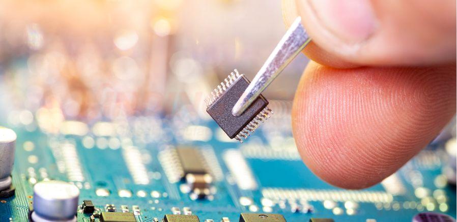
To address this, designers use thermal relief patterns—typically spokes or thin traces—that connect the pad to the plane. These patterns limit the rate at which heat escapes, making it easier to achieve a solid, reliable solder joint. This approach is especially important for through-hole components and high-current paths.
Why Thermal Relief Matters for Soldering and Reliability
The process of soldering relies on controlled heating of both the component lead and the pad to form a strong metallurgical bond. If a pad is connected to a large copper area without any relief, the heat dissipates too quickly, leading to “cold” joints that are weak and unreliable. On the other hand, too little copper connection can result in insufficient current-carrying capacity or poor heat dissipation during operation.
By using thermal relief patterns, designers strike a balance between manufacturability and electrical performance. Properly implemented, these features:
- Ensure consistent, high-quality solder joints during assembly
- Prevent excessive heat buildup at sensitive components
- Maintain adequate electrical connectivity and current flow
- Improve overall reliability and reduce the risk of field failures
For those interested in the broader challenges of making reliable circuits, our article on electronics fabrication challenges provides additional context.
How Thermal Relief Patterns Are Implemented
In PCB layout software, thermal reliefs are typically generated automatically when connecting pads to copper pours or planes. The most common pattern is a set of four thin traces (spokes) radiating from the pad to the plane. The width and number of spokes can be adjusted based on current requirements and the size of the pad.
Key considerations when implementing these features include:
- Current Carrying Needs: High-current connections may require wider or more spokes to prevent overheating during operation.
- Pad Size and Component Type: Larger pads or those for power components often need custom relief patterns.
- Assembly Method: Wave soldering and reflow soldering may have different requirements for effective heat transfer.
- Thermal Simulation: Advanced designs use simulation tools to predict heat flow and optimize relief geometry.
Common Mistakes and Best Practices
While thermal relief is a well-understood concept, mistakes can still occur during design or manufacturing. Some common pitfalls include:
- Omitting reliefs on pads connected to large planes, making soldering difficult
- Using too many or too few spokes, affecting either solderability or current capacity
- Failing to adjust relief patterns for high-power or sensitive analog circuits
- Ignoring manufacturer recommendations or assembly process requirements
To avoid these issues, always review your PCB layout with both the assembly process and operational requirements in mind. Consult your manufacturer’s guidelines and, if possible, run thermal simulations to validate your design choices.
For more on how to verify electrical connections and ensure circuit integrity, see our guide on circuit continuity testing.
Thermal Relief and Broader Thermal Management Strategies
While relief patterns are crucial at the PCB level, they are just one part of a larger strategy for heat control in electronics. Other approaches include heat sinks, thermal vias, careful component placement, and the use of advanced materials. Integrating these methods ensures devices remain within safe operating temperatures, even under demanding conditions.
If you’re designing complex circuits, understanding circuit design rules explained can help you make informed decisions about both electrical and thermal considerations.
Further Learning and Resources
For those seeking a deeper dive into the science and engineering behind heat management in electronics, the electronics tutorials on PCB thermal relief and heat dissipation offer a wealth of diagrams, explanations, and practical examples.
Additionally, learning how to use a multimeter can help you diagnose thermal and electrical issues in your own projects.
Frequently Asked Questions
What is the main purpose of thermal relief in PCB design?
The primary goal is to make soldering easier and more reliable by controlling how quickly heat leaves the pad during assembly. This ensures strong, consistent solder joints without compromising electrical performance.
How do I know if my design needs thermal relief?
If your PCB includes pads connected to large copper planes, especially for through-hole components or high-current paths, you should use relief patterns. Most PCB design software can automatically add these features, but always check your manufacturer’s recommendations.
Can improper thermal relief cause device failure?
Yes. Poorly implemented relief can lead to weak solder joints, increased risk of cold joints, or even overheating during operation. Both manufacturing yield and long-term reliability can be affected.
Are there situations where thermal relief should be avoided?
In some high-current applications, direct connections to copper planes may be necessary for adequate current flow. In these cases, relief patterns may be omitted, but this requires careful consideration of soldering techniques and thermal management.