

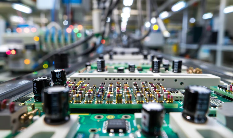
In the world of electronics manufacturing, the quality and reliability of plated surfaces are critical. Plating processes are used to deposit thin layers of metal onto electronic components, providing conductivity, corrosion resistance, and improved solderability. However, various issues can arise during plating, leading to defects that compromise performance and longevity. Understanding these problems, their causes, and how to prevent them is essential for anyone involved in electronics production or quality assurance.
This guide offers a practical overview of common plating issues in electronics, their underlying mechanisms, and effective troubleshooting strategies. Whether you’re a process engineer, quality manager, or simply interested in the intricacies of electronic component manufacturing, you’ll find actionable insights here. For those looking to deepen their understanding of related manufacturing hurdles, you may also want to review our article on electronics fabrication challenges.
Understanding Plating Defects in Electronics
Plating is a controlled electrochemical or chemical process that deposits a thin metal layer onto a substrate, such as a printed circuit board (PCB) or connector pin. The goal is to achieve a uniform, adherent, and defect-free coating. However, several factors can disrupt this process, resulting in visible or hidden flaws. These issues can lead to electrical failures, poor solderability, or even complete device malfunction.
Common plating defects in electronics include roughness, blisters, voids, poor adhesion, and contamination. Each of these problems can stem from a range of sources, such as bath chemistry imbalances, inadequate cleaning, or process control errors. Recognizing the symptoms and root causes is the first step toward effective prevention and remediation.

Types of Plating Defects and Their Causes
Let’s explore the most frequently encountered plating issues in electronics, along with their typical causes and implications for device performance.
Surface Roughness and Nodules
One of the most visible problems is a rough or uneven surface, often accompanied by nodules or bumps. These irregularities can interfere with component assembly and electrical contact.
- Causes: Excessive current density, contaminated plating baths, or poor agitation during the process.
- Impact: Increased contact resistance, unreliable solder joints, and potential for short circuits.
Blistering and Peeling
Blisters are raised areas where the plated layer separates from the substrate. Peeling refers to larger sections of plating lifting away.
- Causes: Inadequate cleaning before plating, trapped gases, or poor adhesion due to improper surface preparation.
- Impact: Loss of electrical continuity, corrosion exposure, and mechanical failure.
Voids and Pitting
Voids are small holes or gaps in the plated layer, while pitting refers to localized corrosion spots. Both can be difficult to detect visually but have serious consequences.
- Causes: Entrapped air, impurities in the plating solution, or inconsistent current distribution.
- Impact: Reduced conductivity, increased risk of corrosion, and compromised reliability.
Contamination and Discoloration
Contaminants in the plating bath or on the substrate can lead to discoloration, dull finishes, or non-uniform coatings.
- Causes: Organic residues, metallic impurities, or inadequate rinsing between process steps.
- Impact: Poor solderability, aesthetic defects, and potential for early failure.

Prevention and Troubleshooting Strategies
Preventing plating defects in electronics requires a combination of process control, regular maintenance, and thorough inspection. Here are some proven strategies:
- Maintain Cleanliness: Ensure all substrates are thoroughly cleaned and degreased before plating. Use deionized water for rinsing to avoid introducing contaminants.
- Monitor Bath Chemistry: Regularly check and adjust the composition of plating solutions. Imbalances in metal ions, pH, or additives can lead to a range of defects.
- Control Process Parameters: Maintain optimal temperature, agitation, and current density. Automated systems can help minimize human error and ensure consistency.
- Inspect and Test: Use visual inspection, cross-section analysis, and electrical testing to catch defects early. Implement statistical process control (SPC) for ongoing monitoring.
- Train Personnel: Ensure operators are well-trained in both the science and practical aspects of plating. Awareness of common pitfalls can help prevent costly mistakes.
For a deeper dive into related topics such as thermal management in electronics, consider exploring additional resources on our blog.
How Plating Defects Affect Electronic Device Performance
Even minor plating flaws can have outsized effects on the performance and reliability of electronic assemblies. Here’s how:
- Electrical Failures: Poor adhesion or voids can interrupt current flow, leading to intermittent or permanent failures.
- Corrosion Vulnerability: Exposed substrate areas or porous coatings allow moisture and contaminants to attack the underlying metal.
- Assembly Issues: Rough or uneven surfaces can prevent proper soldering, resulting in weak joints or open circuits.
- Reduced Lifespan: Devices with plating defects are more likely to fail prematurely, increasing warranty costs and damaging brand reputation.
Addressing these issues early in the manufacturing process is far more cost-effective than dealing with field failures or recalls. For those interested in the broader context of quality assurance in electronics, the electronics tutorials and resources available online provide valuable background and best practices.
Best Practices for Quality Control in Electronics Plating
Implementing robust quality control measures is essential for minimizing plating defects. Consider the following best practices:
- Standardize Procedures: Document and enforce standard operating procedures (SOPs) for every step of the plating process.
- Regular Equipment Maintenance: Keep all tanks, filters, and electrical systems in optimal condition to avoid unexpected process deviations.
- Supplier Quality Management: Work closely with chemical and substrate suppliers to ensure consistent input quality.
- Continuous Improvement: Use root cause analysis and corrective action tracking to address recurring issues and drive ongoing process enhancements.
For those performing hands-on diagnostics, learning how to use a multimeter for electronics testing can be invaluable when verifying the integrity of plated connections.
FAQ: Common Questions About Plating Issues in Electronics
What are the most frequent causes of poor adhesion in electronic plating?
Poor adhesion is often due to inadequate cleaning of the substrate, improper surface activation, or contamination in the plating bath. Ensuring thorough pre-treatment and maintaining bath purity are key preventive measures.
How can manufacturers detect hidden plating defects before assembly?
Non-destructive testing methods such as X-ray inspection, cross-section analysis, and electrical continuity testing can reveal subsurface flaws. Routine visual inspection and adherence to process controls also help catch issues early.
Can plating defects be repaired, or must affected components be scrapped?
Minor surface defects may sometimes be reworked by stripping and re-plating. However, severe issues like extensive blistering or peeling often require scrapping the component to ensure reliability and safety.
Are there industry standards for acceptable plating quality in electronics?
Yes, organizations such as IPC and ASTM provide detailed standards for plating thickness, adhesion, and defect limits. Adhering to these guidelines helps ensure consistent quality and compatibility with downstream processes.
How do plating defects impact solderability?
Defects such as roughness, contamination, or poor adhesion can prevent solder from properly wetting the surface, leading to weak or unreliable solder joints. High-quality plating is essential for robust assembly.
For further reading on related manufacturing and testing topics, explore our guides on circuit continuity testing and circuit design rules explained.