

Ensuring the quality and reliability of electronic products is a top priority in modern manufacturing. As devices become more complex, the need for robust electronics inspection methods grows ever more important. These techniques help manufacturers detect defects, maintain standards, and deliver products that meet customer expectations. In this guide, we’ll break down the most widely used approaches, their advantages, and how they fit into the broader electronics production process.
Whether you’re new to electronics fabrication or looking to refine your quality assurance processes, understanding the available inspection options is essential. For those interested in related manufacturing steps, you might find it helpful to explore how PCB drilling works for a deeper look at upstream production techniques.
Why Inspection Is Critical in Electronics Manufacturing
The intricate nature of electronic assemblies means that even minor defects can lead to significant failures. Inspection serves as a safeguard, catching issues such as soldering errors, component misplacement, or surface contamination before products reach end users. By implementing effective inspection techniques, manufacturers can reduce rework costs, minimize field failures, and uphold their reputation for quality.
Inspection is not a one-size-fits-all process. The choice of method depends on factors like product complexity, production volume, and the types of potential defects. Let’s examine the most common approaches used in the industry today.
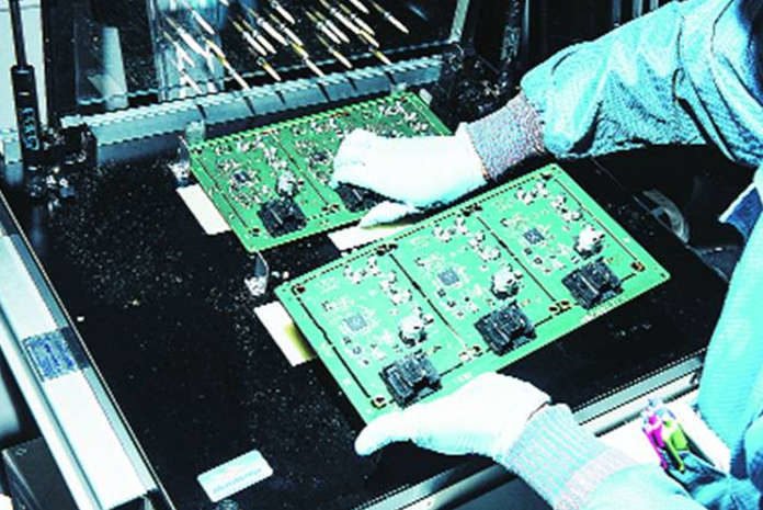
Visual and Manual Examination
The most fundamental form of inspection involves human operators visually checking electronic assemblies. This approach is especially common for low-volume production or prototype runs, where automated systems may not be cost-effective.
- Advantages: Flexible, low initial investment, suitable for catching obvious defects.
- Limitations: Prone to human error, inconsistent results, not scalable for high-volume production.
Manual inspection is often used in conjunction with other methods, serving as a first line of defense or as a final quality check.
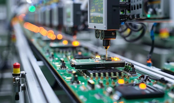
Automated Optical Inspection (AOI)
As production scales up, automated optical inspection becomes a preferred choice. AOI systems use high-resolution cameras and image processing software to scan printed circuit boards (PCBs) for defects such as missing components, solder bridges, or incorrect placements.
- Advantages: Fast, consistent, and capable of detecting a wide range of visual defects.
- Limitations: May miss hidden faults (e.g., under components), requires programming and maintenance.
AOI is typically integrated into the production line, providing real-time feedback and reducing the risk of defective products moving downstream.
Automated X-Ray Inspection (AXI)
For assemblies with dense or hidden solder joints, such as those using Ball Grid Array (BGA) components, automated X-ray inspection is invaluable. AXI systems penetrate the board to reveal internal structures, making it possible to spot voids, cold joints, and other issues invisible to optical methods.
- Advantages: Detects hidden and internal defects, ideal for complex or multilayer boards.
- Limitations: Higher cost, slower than AOI, requires specialized operators.
This technique is often reserved for critical applications or high-value products where reliability is paramount. For more insight into complex board structures, see this resource on how multilayer PCBs are made.
In-Circuit Testing (ICT) and Functional Testing
While visual and X-ray methods focus on physical defects, in-circuit testing (ICT) and functional tests evaluate the electrical performance of assemblies. ICT uses a bed-of-nails fixture to make contact with test points, checking for shorts, opens, and correct component values. Functional testing simulates real-world operating conditions to verify that the device performs as intended.
- Advantages: Confirms electrical integrity, identifies issues not visible to the eye.
- Limitations: Requires custom fixtures and programming, may not catch all latent defects.
Combining ICT and functional testing with other inspection methods creates a comprehensive quality assurance process.
Specialized and Emerging Inspection Approaches
As technology evolves, so do the tools for quality control. Some manufacturers are adopting advanced techniques such as:
- 3D Solder Paste Inspection (SPI): Measures solder paste volume and placement before component mounting.
- Laser Scanning: Provides precise height measurements for components and solder joints.
- Machine Learning and AI: Improves defect detection rates by learning from large datasets of images and test results.
These innovations help address the challenges posed by miniaturization and high-density designs, further enhancing the reliability of electronic products.
Best Practices for Implementing Inspection in Electronics Production
Selecting the right combination of electronics inspection methods depends on your product requirements, production scale, and budget. Here are some best practices to consider:
- Integrate inspection at multiple stages—don’t rely solely on final checks.
- Train staff regularly to recognize new types of defects and use equipment effectively.
- Leverage data from inspection systems to drive process improvements and reduce recurring issues.
- Stay updated on industry standards and emerging technologies to maintain a competitive edge.
For more foundational knowledge on PCB construction and inspection points, the PCB basics tutorial offers a helpful overview.
Additionally, maintaining a safe working environment is crucial. For tips on safety protocols during electronics fabrication, review these electronics fabrication safety tips.
Frequently Asked Questions
What are the most common defects detected by electronics inspection?
Typical issues include solder bridges, missing or misaligned components, insufficient solder, open circuits, and cold solder joints. Advanced inspection can also reveal internal problems like voids under BGAs or micro-cracks in traces.
How do automated inspection systems improve quality control?
Automated systems such as AOI and AXI provide consistent, high-speed analysis that reduces human error and enables early detection of defects. This leads to fewer recalls, lower rework costs, and improved product reliability.
Is it necessary to use multiple inspection methods for every product?
While not always required, combining several inspection techniques—such as visual checks, AOI, and functional testing—offers the most comprehensive coverage. The right mix depends on product complexity, risk tolerance, and production volume.
Conclusion
The landscape of electronics inspection methods is diverse and continually evolving. By understanding the strengths and limitations of each approach, manufacturers can tailor their quality assurance strategies to fit their unique needs. Investing in the right inspection solutions not only protects end users but also strengthens a company’s position in a competitive market.
For further reading on related topics, you may also want to learn about what is impedance control in PCBs or discover practical advice on how to prevent ESD damage during assembly and testing.