

The process of transforming an electronic design into a fully functional product involves a series of carefully coordinated steps. Understanding the electronics fabrication workflow is essential for engineers, hobbyists, and manufacturers alike. This guide breaks down each stage, from initial concept to final assembly, highlighting the tools, materials, and best practices that ensure reliable and efficient results.
Whether you’re new to electronics or looking to refine your manufacturing process, a clear grasp of the fabrication journey can help you avoid common pitfalls and achieve higher quality outcomes. For those interested in the origins of individual parts, you may also want to explore how electronics components are made for deeper insight into the materials and processes behind each component.
Key Steps in the Electronics Manufacturing Process
A typical electronics fabrication workflow can be divided into several main phases. Each phase builds upon the previous one, ensuring that the final product meets design requirements and industry standards.
- Design and schematic capture
- PCB layout and design verification
- Material selection and procurement
- PCB fabrication
- Component assembly
- Testing and quality assurance
- Final assembly and packaging
From Concept to Schematic: The Design Phase
Every electronic device starts with an idea. The first step is to translate this idea into a practical circuit using schematic capture tools. Engineers select appropriate components, define electrical connections, and simulate circuit behavior to ensure functionality. This phase is critical, as errors here can propagate through the entire workflow.
During schematic design, attention is paid to signal integrity, power distribution, and component compatibility. Modern tools allow for simulation and validation before moving to the next step, reducing the risk of costly revisions later.
PCB Layout and Design Verification
Once the schematic is finalized, the next task is to create the physical layout of the printed circuit board (PCB). This involves placing components, routing traces, and defining board layers. Design verification checks are performed to catch issues like trace width violations, clearance errors, or unconnected nets.
For those interested in hands-on approaches, the DIY PCB fabrication guide provides practical tips for beginners tackling their own layouts.
Material Selection and Procurement in the Workflow
Selecting the right materials is a crucial part of the electronics fabrication workflow. This includes choosing the PCB substrate, copper thickness, solder mask, and silkscreen materials. Additionally, sourcing reliable electronic components ensures consistent performance and reduces the risk of defects.
Procurement teams work closely with suppliers to secure parts that meet the required specifications and delivery timelines. Shortages or counterfeit components can disrupt production, so careful vetting and inventory management are essential.
PCB Fabrication: Turning Designs into Boards
The PCB fabrication stage transforms digital layouts into physical boards. This process typically involves several steps:
- Printing the circuit pattern onto copper-clad boards
- Etching away excess copper to form traces
- Drilling holes for through-hole components and vias
- Applying solder mask and silkscreen
- Surface finishing (e.g., HASL, ENIG) to protect exposed pads
Quality control at this stage is vital. Any defects in the board can lead to failures during assembly or operation. Automated optical inspection (AOI) and electrical testing are commonly used to verify board integrity.
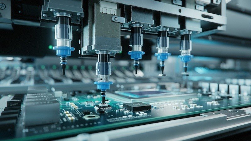
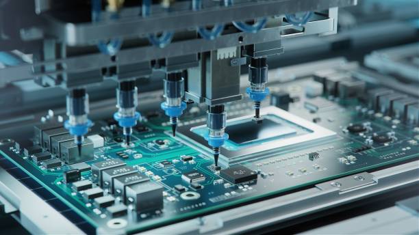
Component Assembly and Soldering Techniques
With the boards ready, the next step is to mount components. This can be done using surface-mount technology (SMT), through-hole assembly, or a combination of both. Automated pick-and-place machines position components with high precision, followed by soldering processes such as reflow or wave soldering.
For a deeper dive into soldering processes, see the detailed explanation of how wave soldering works in PCB assembly.
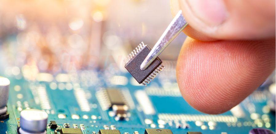
Manual assembly is still used for prototypes or low-volume runs, while high-volume production relies on automation. After soldering, boards are cleaned to remove flux residues and inspected for defects.
Testing and Quality Assurance in Electronics Production
Rigorous testing ensures that assembled boards function as intended. This phase may include in-circuit testing (ICT), functional testing, and environmental stress screening. Detecting issues early prevents defective products from reaching customers.
For more information about common test methods, refer to the article on electronics testing methods.
Quality assurance teams document test results and implement corrective actions for recurring problems. This continuous improvement approach helps maintain high standards and customer satisfaction.
Final Assembly, Packaging, and Shipping
The last stage involves integrating the tested PCBs into their enclosures, attaching connectors, and performing final inspections. Proper packaging protects sensitive electronics from static, moisture, and mechanical damage during transit.
Shipping logistics are coordinated to ensure timely delivery to customers or distributors. Traceability systems track each unit, supporting warranty claims and recalls if necessary.
Best Practices for a Smooth Fabrication Workflow
To optimize the electronics fabrication workflow, consider the following recommendations:
- Start with a clear, validated design to minimize revisions
- Use reputable suppliers for components and materials
- Automate repetitive tasks where possible to reduce errors
- Implement robust testing at multiple stages
- Maintain thorough documentation for traceability and compliance
- Continuously review and improve processes based on feedback
For those assembling circuits by hand or in small batches, having the right circuit prototyping materials can make a significant difference in quality and efficiency.
Further Learning and Resources
The field of electronics manufacturing is vast and constantly evolving. Staying updated with industry trends, new materials, and emerging technologies is crucial. For foundational knowledge and tutorials, comprehensive electronics tutorials offer valuable insights into circuit theory, components, and practical applications.
Frequently Asked Questions
What is the most critical step in the electronics manufacturing process?
Each phase plays a vital role, but the design and schematic capture stage is often considered the most critical. Errors made here can lead to costly revisions and failures later in the workflow. Thorough validation and simulation at this stage help ensure a smooth process downstream.
How can defects be minimized during PCB fabrication?
Defects can be reduced by using high-quality materials, following precise manufacturing protocols, and implementing automated inspection methods such as AOI and electrical testing. Regular process audits and staff training also contribute to higher yields and fewer errors.
Why is testing important in electronics production?
Testing verifies that each product meets functional and safety standards before reaching the customer. It helps identify issues early, prevents defective units from being shipped, and supports continuous improvement in manufacturing processes.