

Understanding electronics fabrication basics is essential for anyone interested in how modern electronic devices are designed and produced. From the smallest sensors to complex computing systems, the journey from concept to finished product involves several precise and interconnected steps. This guide offers a clear overview of the fundamental processes, materials, and quality checks that define the world of electronics manufacturing.
Whether you’re a student, a hobbyist, or a professional looking to refresh your knowledge, learning about the core stages of fabrication can help you appreciate the complexity behind everyday technology. For those interested in broader industry trends, exploring topics like hardware design trends and innovations can provide valuable context for how fabrication methods continue to evolve.
Key Steps in Modern Electronics Manufacturing
The process of creating electronic products involves a sequence of carefully managed steps, each critical to the final outcome. Below is a breakdown of the primary stages that make up the foundation of electronics fabrication basics:
- Design and Schematic Capture: Engineers begin by drafting circuit diagrams and selecting components that will meet the device’s requirements.
- PCB Layout: The schematic is translated into a physical layout, determining where each component will be placed on the printed circuit board (PCB).
- Fabrication of the PCB: The board is manufactured using processes such as etching, drilling, and plating to create the necessary pathways for electrical signals.
- Component Mounting: Components are attached to the PCB using either through-hole or surface-mount technology (SMT).
- Soldering: Automated or manual soldering secures components and ensures reliable electrical connections.
- Testing and Inspection: Each assembly is checked for defects and functionality using a range of test methods.
- Final Assembly and Packaging: The completed boards are integrated into their housings and prepared for shipment.
Materials and Tools Used in Fabrication
The choice of materials and equipment directly impacts the quality and reliability of electronic assemblies. Here are some essentials used throughout the fabrication process:
- Substrates: Most PCBs are made from fiberglass-reinforced epoxy (FR4), valued for its durability and electrical insulation properties.
- Copper Foil: Thin layers of copper are laminated onto the substrate to form conductive traces.
- Solder Paste: A mixture of powdered metal and flux, applied to pads before component placement.
- Pick-and-Place Machines: Automated systems that position components with high precision.
- Reflow Ovens: Used to melt solder paste and permanently attach components during SMT assembly.
- Inspection Tools: Microscopes, X-ray machines, and automated optical inspection (AOI) systems help identify defects.

Understanding PCB Assembly Techniques
Two primary methods are used to attach components to circuit boards: through-hole and surface-mount technology. Each has its own advantages and is chosen based on the application’s requirements.
- Through-Hole Assembly: Components with leads are inserted into holes drilled in the PCB and soldered on the opposite side. This method provides strong mechanical bonds and is often used for connectors or large parts.
- Surface-Mount Technology (SMT): Components are placed directly onto the surface of the board. SMT allows for smaller, denser assemblies and is the standard for most modern electronics.
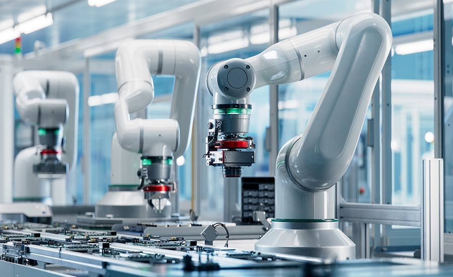
Automated assembly lines, such as those shown below, have revolutionized the speed and consistency of electronics production.

Quality Control and Testing in Electronics Fabrication
Ensuring the reliability of electronic assemblies is a top priority. Multiple testing and inspection steps are integrated into the fabrication workflow to catch defects early and guarantee performance.
- Automated Optical Inspection (AOI): Cameras scan the boards for misplaced or missing components and soldering issues.
- In-Circuit Testing (ICT): Electrical probes check the integrity of connections and component values.
- Functional Testing: The completed assembly is powered up and tested to verify it performs as intended.
- X-ray Inspection: Used to examine hidden solder joints, especially for components like BGAs (Ball Grid Arrays).
For a deeper dive into the various test methods for electronic components, industry resources provide comprehensive overviews of the latest standards and best practices.
Common Challenges and Best Practices
Even with advanced tools and processes, electronics manufacturing faces several challenges. Here are some common issues and practical tips for addressing them:
- Component Sourcing: Supply chain disruptions can delay production. Building relationships with multiple suppliers and maintaining buffer stock can help mitigate risks.
- Design for Manufacturability (DFM): Early consideration of manufacturing constraints during design reduces costly revisions and improves yield.
- Thermal Management: High-density boards can overheat. Incorporating heat sinks, thermal vias, and proper layout techniques helps manage temperature.
- Prototyping and Feedback: Rapid prototyping and early testing allow teams to identify and resolve issues before full-scale production. For more on this, see the importance of early prototyping feedback.
- Troubleshooting: Systematic debugging and the use of diagnostic tools are crucial for resolving unexpected problems. Guidance on how to troubleshoot hardware prototypes can be particularly helpful for new engineers.
Integrating Fabrication into the Product Lifecycle
The fabrication phase is just one part of a larger product development journey. Effective coordination between design, prototyping, fabrication, and testing ensures that products reach the market faster and with fewer defects. Teams often follow a structured hardware engineering project workflow to manage these interconnected steps efficiently.
As technology advances, new materials, automation, and quality control methods continue to shape the landscape of electronics manufacturing. Staying informed about these developments helps engineers and organizations maintain a competitive edge.
Frequently Asked Questions
What is the difference between PCB fabrication and PCB assembly?
PCB fabrication refers to the process of manufacturing the bare circuit board, including creating the substrate, etching copper traces, and drilling holes. PCB assembly, on the other hand, involves mounting and soldering electronic components onto the fabricated board to create a functional device.
Why is surface-mount technology preferred in modern electronics?
Surface-mount technology (SMT) allows for smaller, lighter, and more densely packed circuit boards. It supports automated assembly, which increases production speed and consistency while reducing costs compared to traditional through-hole methods.
How do manufacturers ensure the quality of electronic assemblies?
Quality is maintained through a combination of automated inspections, electrical testing, and functional verification. Techniques such as AOI, ICT, and X-ray inspection help detect defects early, while functional tests confirm that the final product meets design specifications.