

The copper plating process is a fundamental technique in electronics manufacturing, metal finishing, and various industrial applications. It involves depositing a thin layer of copper onto the surface of another material, typically to enhance electrical conductivity, improve corrosion resistance, or prepare components for further processing. Understanding the steps, chemistry, and best practices behind copper electroplating is essential for engineers, technicians, and anyone interested in modern fabrication techniques.
In this guide, we’ll break down each stage of the process, highlight its importance in industries like printed circuit board (PCB) fabrication, and provide practical insights for achieving high-quality results. For those curious about related manufacturing steps, you can also explore how PCB drilling works to see how copper plating fits into the broader context of electronics production.
What Is Copper Electroplating?
At its core, copper electroplating is an electrochemical process where copper ions in a solution are reduced and deposited onto a conductive substrate. The process uses an electrical current to drive the movement of copper from a source (anode) to the item being plated (cathode). This technique is widely used for coating metals and non-metals, especially in the electronics sector for creating conductive pathways on PCBs.
The versatility of copper plating makes it valuable not only for electronics but also for decorative finishes, corrosion protection, and as a preparatory layer for further metal coatings such as nickel or tin.
Key Steps in the Copper Plating Workflow
Achieving a uniform and reliable copper layer requires careful attention to each stage of the process. Here’s a step-by-step overview:
- Surface Preparation: The substrate must be thoroughly cleaned to remove oils, oxides, and contaminants. This often involves degreasing, acid cleaning, and rinsing to ensure optimal adhesion.
- Activation: For non-conductive materials or complex geometries, an activation step (such as a thin conductive seed layer) may be necessary to initiate plating.
- Electrolyte Bath Preparation: The plating bath contains copper sulfate, sulfuric acid, and various additives to control deposit quality. Temperature, pH, and agitation are carefully managed.
- Electroplating: The workpiece (cathode) and a copper anode are immersed in the bath. A direct current is applied, causing copper ions to migrate and deposit onto the substrate.
- Post-Plating Treatment: After plating, the part is rinsed to remove residual chemicals and may undergo further treatments such as annealing or passivation to enhance properties.
- Inspection and Quality Control: The final product is inspected for thickness, adhesion, and surface finish to ensure it meets specifications.
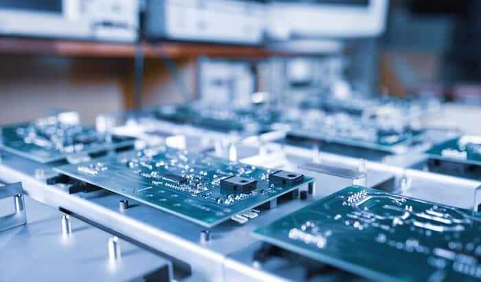
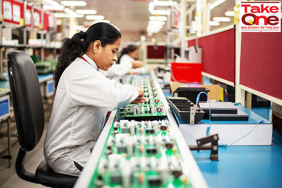
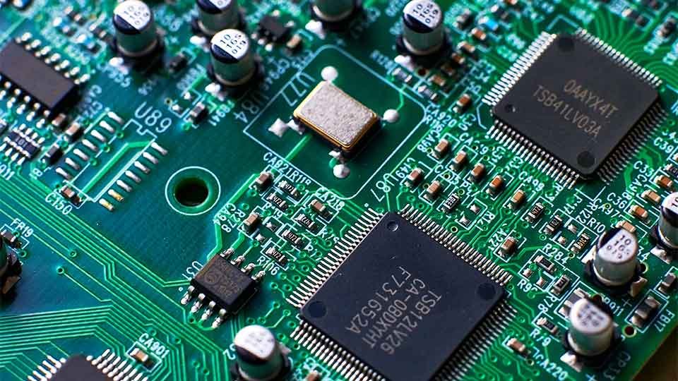
Applications of Copper Plating in Electronics
The use of copper plating is especially prominent in the fabrication of printed circuit boards. In PCB manufacturing, copper layers form the conductive tracks that connect components and enable electronic functionality. The process is also used to create vias—tiny holes plated with copper that allow signals to pass between layers in multilayer boards.
Beyond PCBs, copper plating is used in connectors, semiconductors, and various microelectronic devices. For a deeper look at advanced electronics production, see this comprehensive guide to semiconductor fabrication processes.
Critical Factors for High-Quality Copper Deposition
Producing a defect-free copper layer requires attention to several variables:
- Bath Composition: The concentration of copper ions, acid, and additives directly affects deposit quality and plating speed.
- Current Density: Too high or too low a current can cause uneven plating, burning, or poor adhesion.
- Temperature Control: Stable temperatures ensure consistent plating rates and reduce stress in the deposit.
- Agitation: Proper agitation prevents buildup of byproducts and ensures uniform ion distribution.
- Substrate Preparation: Inadequate cleaning or surface defects can lead to peeling, pitting, or poor coverage.
For those working with advanced circuit designs, understanding what is impedance control in PCBs can be crucial, as copper thickness and uniformity directly impact electrical performance.
Common Challenges and Troubleshooting Tips
Even with careful control, several issues can arise during copper electroplating. Here are some typical problems and their solutions:
- Poor Adhesion: Often caused by inadequate cleaning or surface preparation. Ensure all contaminants are removed before plating.
- Rough or Dull Deposits: May result from improper bath chemistry or low agitation. Regularly monitor solution composition and maintain proper agitation.
- Pitting or Pinholes: Usually due to trapped gases or particles on the surface. Use thorough rinsing and filtration to minimize defects.
- Non-uniform Thickness: Can be caused by uneven current distribution or poor part positioning. Adjust racking and use auxiliary anodes if necessary.
For those interested in safety and best practices during fabrication, the article on electronics fabrication safety tips offers valuable guidance for working with chemicals and electrical equipment.
Environmental and Safety Considerations
The chemicals used in copper plating, such as acids and metal salts, require careful handling and disposal. Facilities must comply with environmental regulations to prevent contamination and protect workers. Proper ventilation, personal protective equipment, and waste treatment systems are essential components of a responsible plating operation.
Additionally, many manufacturers are exploring alternative processes and greener chemistries to minimize environmental impact while maintaining high-quality results.
Frequently Asked Questions
What materials can be copper plated?
Copper can be deposited onto a wide range of materials, including metals like steel, aluminum, and brass, as well as certain plastics and ceramics. For non-conductive materials, a conductive seed layer is typically applied before plating.
How thick is the typical copper layer in electronics manufacturing?
In PCB fabrication, copper thickness can vary from a few microns (for fine traces) to several tens of microns (for power applications). The required thickness depends on the application, current-carrying needs, and design specifications.
Is copper plating environmentally friendly?
While copper itself is not highly toxic, the chemicals used in the process can pose environmental risks if not managed properly. Many facilities invest in advanced waste treatment and recycling systems to reduce their environmental footprint.
What are some alternatives to copper plating?
Alternatives include electroless nickel plating, tin plating, and other metal deposition techniques. However, copper remains the preferred choice for many electronic and industrial applications due to its excellent conductivity and cost-effectiveness.
Conclusion
Mastering the copper plating process is essential for anyone involved in electronics manufacturing, metal finishing, or industrial fabrication. By understanding each step—from surface preparation to quality control—and being aware of common challenges, you can achieve reliable, high-performance copper coatings. For those interested in exploring further, topics like how multilayer PCBs are made and how to prevent ESD damage provide additional context for advanced electronics production.