

In modern electronics, the precise management of electrical signals is essential for reliable device performance. One of the most important techniques used to achieve this is controlled impedance routing. This method ensures that signal traces on printed circuit boards (PCBs) maintain a consistent impedance, which is critical for high-speed data transmission and minimizing signal integrity issues such as reflections, noise, and data loss.
As electronic devices become faster and more complex, understanding the principles behind impedance control is increasingly important for engineers, designers, and manufacturers. This article provides a practical overview of the topic, including why it matters, how it is implemented, and the challenges involved. For those interested in related manufacturing processes, you may also want to explore electronics fabrication challenges for further context on the broader production landscape.
Understanding Signal Integrity and Impedance
At its core, impedance is the total opposition that a circuit presents to the flow of alternating current (AC). In the context of PCBs, it is determined by the trace width, the thickness and type of dielectric material, the distance between traces, and the presence of ground planes. Maintaining a consistent impedance is crucial for high-frequency signals, as even small variations can cause reflections and degrade signal quality.
Signal integrity refers to the preservation of the quality and timing of electrical signals as they travel through a circuit. When impedance is not properly controlled, signals can become distorted, leading to errors, data corruption, or even device failure. This is particularly important in applications such as telecommunications, computing, and automotive electronics, where high-speed data transfer is the norm.
Why Impedance Control Matters in PCB Design
As data rates increase, the wavelength of signals becomes comparable to the physical dimensions of PCB traces. In these scenarios, traces act as transmission lines rather than simple wires. If the impedance of these lines is not matched to the source and load, part of the signal is reflected back, causing interference and loss of signal integrity.
Controlled impedance routing ensures that each trace maintains a specified impedance, typically 50 or 100 ohms, depending on the application. This is achieved by carefully designing the trace geometry and the PCB stack-up. The benefits include:
- Reduced signal reflections and improved data accuracy
- Minimized electromagnetic interference (EMI)
- Reliable operation at higher frequencies
- Compliance with industry standards for high-speed interfaces
For a deeper dive into the foundational rules that support these practices, reviewing circuit design rules explained can provide valuable context.
Key Factors Affecting Controlled Impedance
Achieving precise impedance control involves several interrelated factors. The most significant include:
- Trace width and thickness: Wider or thicker traces have lower impedance, while narrower or thinner traces have higher impedance.
- Dielectric constant (Dk): The material between the trace and the reference plane affects how signals propagate. Materials with a higher Dk reduce impedance.
- Distance to reference plane: The closer a trace is to a ground or power plane, the lower its impedance.
- Trace configuration: Single-ended and differential pairs require different design approaches to maintain consistent impedance.
Designers use specialized software to calculate and simulate these parameters, ensuring that the final PCB meets the required specifications. Manufacturing tolerances must also be considered, as small deviations can impact performance.
Best Practices for High-Speed Routing
Implementing effective impedance control requires attention to detail throughout the design and manufacturing process. Here are some best practices:
- Work closely with your PCB manufacturer to understand their capabilities and tolerances.
- Use impedance calculators or field solvers to model your trace geometry before finalizing the layout.
- Maintain consistent trace widths and spacing, especially for differential pairs.
- Minimize stubs and avoid sharp corners, which can cause impedance discontinuities.
- Document all impedance requirements clearly in your fabrication notes.
These steps help ensure that the finished board performs as expected, reducing the risk of costly revisions or failures in the field.
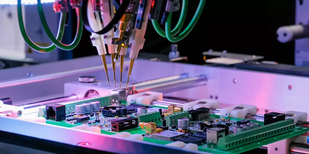
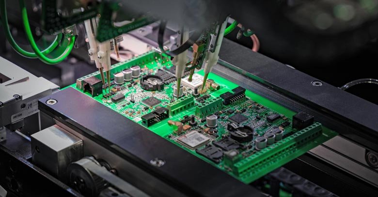
Manufacturing Considerations and Quality Control
Even with careful design, the manufacturing process introduces variables that can affect impedance. Factors such as etching accuracy, material consistency, and layer alignment all play a role. To address these, manufacturers often use test coupons—small sections of the PCB fabricated alongside the main board—to measure and verify impedance during production.
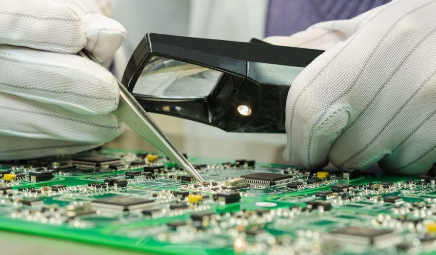
Quality control is critical. If the measured impedance falls outside the specified range, adjustments may be needed before full-scale production. This iterative approach helps maintain high standards and ensures that the final product meets performance requirements.
For those interested in the broader context of electronics production, the electronics manufacturing process overview provides a comprehensive look at the steps involved from design to finished product.
Common Challenges in Achieving Consistent Impedance
While the principles of impedance control are well understood, practical implementation can be challenging. Some of the most common issues include:
- Material variability: Differences in dielectric properties between batches can affect impedance.
- Manufacturing tolerances: Small deviations in trace width or spacing can lead to significant impedance changes.
- Complex stack-ups: Multi-layer boards with mixed signal types require careful planning to avoid crosstalk and maintain control.
- Cost considerations: High-precision materials and processes can increase manufacturing costs.
Addressing these challenges requires collaboration between designers, engineers, and manufacturers, as well as thorough testing and validation.
Applications That Depend on Impedance Control
Many advanced electronic systems rely on precise impedance management for optimal performance. Examples include:
- High-speed data interfaces (USB, HDMI, PCIe, Ethernet)
- RF and microwave circuits
- Telecommunications equipment
- Automotive and aerospace electronics
- Medical devices with sensitive signal requirements
In these applications, even minor signal degradation can have significant consequences, making controlled routing an essential aspect of design.
Frequently Asked Questions
What is the main purpose of controlled impedance routing?
The primary goal is to ensure that signal traces on a PCB maintain a consistent impedance, which is vital for preserving signal integrity and preventing issues like reflections, noise, and data loss in high-speed circuits.
How do designers calculate the correct impedance for PCB traces?
Designers use specialized software tools and impedance calculators that take into account trace width, thickness, dielectric constant, and distance to reference planes. These calculations are verified through simulation and often validated with test coupons during manufacturing.
What happens if impedance is not controlled in a high-speed PCB?
Without proper impedance management, signals can reflect or become distorted, leading to errors, data corruption, and reduced device reliability. This is especially problematic in applications where high-frequency or high-speed data transmission is required.
For more insights into related topics, you might find our articles on thermal management in electronics and how to use a multimeter useful for understanding other critical aspects of electronic system design.