

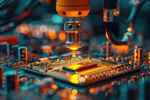
The integration of 3D printing for electronics is transforming how engineers and manufacturers approach the design and production of electronic devices. By enabling rapid prototyping, custom geometries, and the direct embedding of conductive materials, additive manufacturing is opening new possibilities for innovation in the electronics sector. Whether you are developing printed circuit boards (PCBs), sensors, or custom enclosures, understanding the capabilities and limitations of this technology is essential for anyone involved in electronics design and manufacturing.
As the demand for smaller, more complex, and highly functional electronic devices grows, additive manufacturing offers a flexible and efficient solution. This article explores the fundamentals, practical steps, and real-world applications of using 3D printing in electronics, providing a comprehensive guide for professionals and enthusiasts alike. For those interested in related challenges, you may also want to explore electronics fabrication challenges to understand the broader context of modern electronics production.
Understanding Additive Manufacturing in Electronics
Additive manufacturing, often referred to as 3D printing, involves building objects layer by layer from digital models. In the context of electronics, this approach allows for the creation of complex structures, including the integration of conductive and insulating materials within a single print. Unlike traditional subtractive methods, which remove material to achieve the desired shape, additive processes minimize waste and enable rapid iteration.
There are several methods used in 3D printing for electronics, including:
- Fused Deposition Modeling (FDM): Commonly used for prototyping enclosures and non-conductive parts.
- Inkjet Printing: Allows for the deposition of conductive inks to create traces and circuits directly onto substrates.
- Aerosol Jet Printing: Suitable for fine-feature electronics and flexible circuits.
- Stereolithography (SLA): Used for high-resolution components and microfluidic devices.

Key Benefits of 3D Printing in Electronic Device Development
The adoption of additive manufacturing in electronics brings several significant advantages:
- Rapid Prototyping: Engineers can quickly produce and test new designs, reducing development cycles from weeks to days.
- Customization: Tailored enclosures, connectors, and circuit layouts can be produced on demand, supporting unique project requirements.
- Integration: Conductive materials can be embedded alongside insulators, enabling the direct printing of functional circuits and sensor arrays.
- Material Efficiency: Additive processes use only the material needed, minimizing waste and lowering costs.
- Complex Geometries: Designs that are impossible or impractical with traditional manufacturing can be realized, such as conformal circuits or internal channels for cooling.
These benefits make 3D printing for electronics especially attractive for research and development, low-volume production, and applications where agility and innovation are critical.
Common Applications of Additive Manufacturing in Electronics
The use of 3D printing in electronics spans a wide range of applications, from consumer products to industrial systems. Some of the most notable uses include:
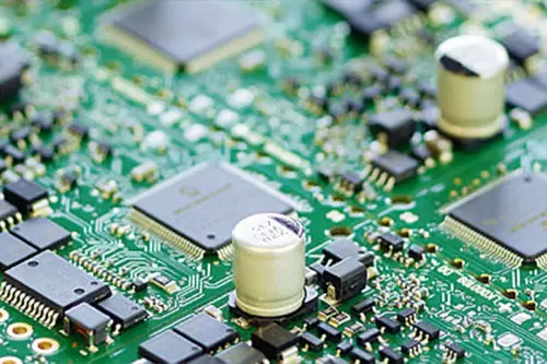
- Printed Circuit Boards (PCBs): Directly printing conductive traces and insulating layers to create functional prototypes or small production runs.
- Custom Enclosures: Designing and producing cases that perfectly fit unique components or form factors.
- Antennas and RF Devices: Fabricating complex antenna structures for wireless communication devices.
- Wearable Electronics: Creating flexible, lightweight devices for integration into clothing or accessories.
- Sensors and Actuators: Printing integrated sensor arrays or micro-electromechanical systems (MEMS).
- Thermal Management: Developing heat sinks and cooling channels directly within device enclosures, which ties into broader topics like thermal management in electronics.
Step-by-Step Guide to Using 3D Printing for Electronics Projects
Implementing additive manufacturing in electronics involves several key steps. Here’s a practical overview for those looking to get started:
- Define the Application: Determine whether you need to print a PCB, enclosure, sensor, or another component. Consider the required electrical and mechanical properties.
- Select Suitable Materials: Choose from conductive inks, thermoplastics, resins, or flexible polymers based on your design needs. Material compatibility is crucial for both performance and reliability.
- Design the Model: Use CAD software to create a digital model of your component. For circuits, ensure trace widths and spacing meet electrical requirements and circuit design rules explained in industry standards.
- Prepare for Printing: Slice the model and set up the printer with the correct materials. For multi-material prints, ensure proper alignment and calibration.
- Print and Post-Process: Run the print job, then perform any necessary post-processing steps such as curing, soldering, or assembly.
- Test and Validate: Use appropriate methods to check electrical continuity, insulation, and overall functionality. For more on this, see how to use a multimeter for electronics testing.
Each step may require iteration, especially during prototyping. The flexibility of 3D printing allows for quick adjustments and reprints, making it ideal for experimental and custom projects.
Challenges and Considerations in Additive Electronics Manufacturing
While the advantages are clear, there are also challenges to address when using additive manufacturing for electronic components:
- Material Limitations: Not all conductive inks or printable polymers offer the same performance as traditional materials. Conductivity, adhesion, and long-term stability can vary.
- Resolution and Precision: Fine features required for high-frequency circuits or dense PCBs may exceed the capabilities of some 3D printers.
- Testing and Quality Assurance: Ensuring the reliability of printed electronics requires thorough inspection and validation. For a deeper look at component testing, see this overview of test methods for electronic components.
- Cost and Scalability: While ideal for prototyping and short runs, 3D printing may not always be cost-effective for mass production compared to established manufacturing methods.
- Standards Compliance: Meeting industry standards for safety, electromagnetic compatibility, and durability is essential, especially for commercial products.
Addressing these challenges often involves a combination of careful material selection, design optimization, and rigorous testing procedures.
Future Trends in 3D-Printed Electronics
The field of 3D printing for electronics continues to evolve rapidly. Emerging trends include the integration of more advanced materials, such as nanomaterials and flexible substrates, which enable the creation of stretchable and wearable devices. Hybrid manufacturing approaches, combining additive and traditional processes, are also gaining traction for producing complex assemblies.
Automation and improved printer precision are expanding the range of possible applications, from biomedical sensors to aerospace electronics. As research progresses, expect to see greater adoption of additive manufacturing in mainstream electronics production, especially for applications requiring customization, rapid iteration, or unique geometries.
Frequently Asked Questions
What types of materials can be used for 3D-printed electronics?
Materials commonly used include conductive inks (silver, copper, carbon-based), thermoplastics like ABS and PLA for structural parts, flexible polymers for wearable devices, and specialized resins for high-resolution features. The choice depends on the application’s electrical, thermal, and mechanical requirements.
How does 3D printing benefit the prototyping of electronic devices?
Additive manufacturing allows for rapid iteration of designs, enabling engineers to test and refine prototypes quickly. This reduces development time and costs, while supporting the creation of custom or complex components that would be difficult to produce with traditional methods.
Are 3D-printed electronic components as reliable as traditional ones?
Reliability depends on materials, printer precision, and post-processing. While 3D-printed prototypes are excellent for testing and low-volume production, mass-produced components often require additional validation to meet industry standards for durability and performance.