


Signal interference is a persistent challenge in electronics, affecting everything from simple hobby projects to advanced industrial systems. Unwanted noise or crosstalk can degrade performance, cause data errors, or even lead to complete circuit failure. Understanding how to avoid signal interference is essential for anyone involved in designing, assembling, or troubleshooting electronic circuits.
Whether you’re working on a printed circuit board (PCB) or a breadboard prototype, minimizing interference requires a combination of good design practices, careful component selection, and proper assembly methods. In this article, we’ll explore practical strategies to reduce noise, prevent crosstalk, and maintain signal integrity throughout your circuit.
For those interested in the finer points of PCB design, understanding what are test points can also play a role in diagnosing and mitigating interference issues early in the development process.
Understanding the Causes of Signal Disturbance
Before diving into solutions, it’s important to recognize what causes unwanted noise and disruption in electronic circuits. Common sources include electromagnetic interference (EMI), radio frequency interference (RFI), ground loops, and improper layout. Each of these can introduce unwanted voltages or currents that disrupt normal signal flow.
- Electromagnetic interference (EMI): Generated by nearby electronic devices, motors, or switching power supplies.
- Radio frequency interference (RFI): Caused by radio transmitters, wireless devices, or even poorly shielded cables.
- Ground loops: Occur when there are multiple ground paths, leading to circulating currents and voltage differences.
- Crosstalk: Signals from one trace or wire induce unwanted signals in adjacent traces or wires.
Recognizing these sources is the first step toward implementing effective countermeasures and ensuring reliable circuit operation.
Best Practices for Minimizing Interference in Circuit Design
The foundation of any robust electronic system lies in its design. By following proven layout and routing techniques, you can significantly reduce the risk of signal degradation.
Optimizing PCB Layout to Prevent Signal Issues
A well-planned PCB layout is crucial for minimizing noise. Here are some essential tips:
- Keep signal traces short and direct: Long traces act as antennas, picking up unwanted signals.
- Separate analog and digital sections: Digital circuits generate fast switching noise that can affect sensitive analog components.
- Use ground planes: A continuous ground plane beneath signal traces provides a low-impedance return path, reducing EMI susceptibility.
- Route high-speed signals carefully: Avoid sharp angles and parallel runs with other traces to minimize crosstalk.
- Decouple power supply lines: Place decoupling capacitors close to IC power pins to filter out high-frequency noise.
For more details on how vias and copper plating can affect signal integrity, you may want to review resources like how vias are made in PCBs and copper plating process explained.
Shielding and Grounding Techniques
Proper shielding and grounding are among the most effective ways to block external noise and contain internal emissions.
- Enclose sensitive circuits: Use metal enclosures or shields to block external EMI and RFI.
- Connect shields to ground: Ensure that any shielding is properly connected to the main ground point to avoid floating potentials.
- Implement single-point grounding: Use a star ground configuration to prevent ground loops and circulating currents.
- Isolate noisy components: Physically separate high-power or high-frequency parts from low-level analog sections.
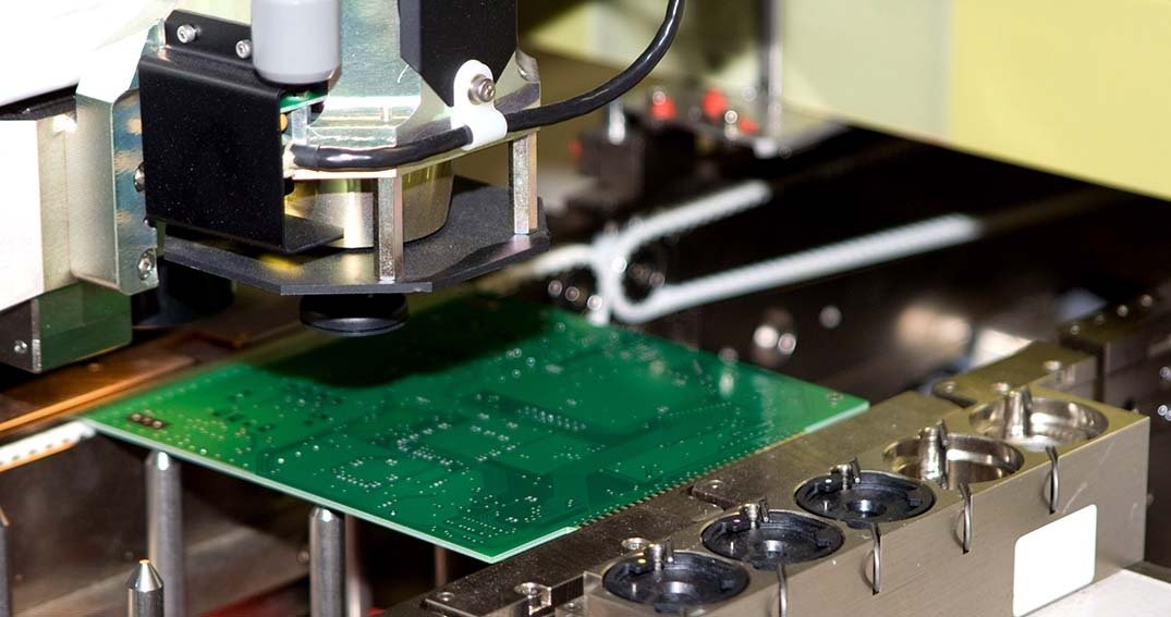
Assembly and Manufacturing Tips to Reduce Noise
Even the best-designed circuits can suffer from interference if not assembled with care. Paying attention to assembly details can make a significant difference.
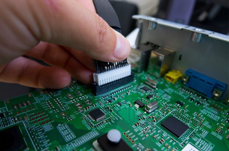
Component Placement and Soldering
Placing components in the correct orientation and position helps maintain signal integrity:
- Group related components: Keep components that interact closely together to minimize trace lengths.
- Maintain consistent orientation: Align components to simplify routing and reduce the chance of accidental crosstalk.
- Use proper soldering techniques: Cold or cracked solder joints can introduce resistance and act as antennas for noise.
For those new to electronics assembly, resources like this beginner’s guide to electronics projects provide practical advice on manual assembly and best practices to avoid common pitfalls.
Testing and Inspection for Signal Integrity
After assembly, thorough testing is vital to ensure that no unexpected interference has crept into the circuit. Use oscilloscopes, logic analyzers, or spectrum analyzers to check for noise on critical signals. Automated inspection methods, discussed in detail in electronics inspection methods, can help identify subtle issues that might otherwise go unnoticed.
Practical Steps for Troubleshooting Interference
If you encounter unexpected noise or erratic behavior in your circuit, a systematic troubleshooting approach can help identify and resolve the issue:
- Visual inspection: Check for poor solder joints, damaged traces, or misplaced components.
- Check grounding: Verify that all ground connections are solid and that there are no unintended loops.
- Probe signal paths: Use an oscilloscope to look for noise spikes or oscillations on key signals.
- Isolate sections: Temporarily disconnect or shield parts of the circuit to pinpoint the source of interference.
- Review layout: Compare your PCB or wiring layout against best practices to spot potential problem areas.
Frequently Asked Questions
What are the most common sources of signal interference in electronic circuits?
The most frequent sources include electromagnetic interference from nearby devices, radio frequency emissions, ground loops, and improper PCB layout. High-speed digital signals and power supplies can also introduce noise if not managed carefully.
How can I shield my circuit from external noise?
Using metal enclosures or shields connected to a solid ground can block external electromagnetic and radio frequency interference. Additionally, keeping sensitive traces short and using ground planes on your PCB help contain and redirect unwanted signals.
What role does PCB layout play in preventing signal problems?
PCB layout is critical for maintaining signal integrity. Proper trace routing, separation of analog and digital sections, use of ground planes, and careful placement of decoupling capacitors all contribute to minimizing interference and ensuring reliable circuit operation.