

Creating a reliable and efficient electronic device starts with a well-planned layout. Whether you are designing a simple circuit or a complex printed circuit board (PCB), the way you arrange components and route traces can significantly impact performance, manufacturability, and long-term reliability. This guide covers essential electronics layout tips to help you avoid common pitfalls, streamline your workflow, and achieve professional results.
Before diving into specific strategies, it’s important to understand that a thoughtful layout is more than just placing parts on a board. It involves considering signal integrity, thermal management, manufacturability, and future testing needs. By following proven techniques, you can reduce errors, minimize rework, and ensure your project meets both functional and production requirements.

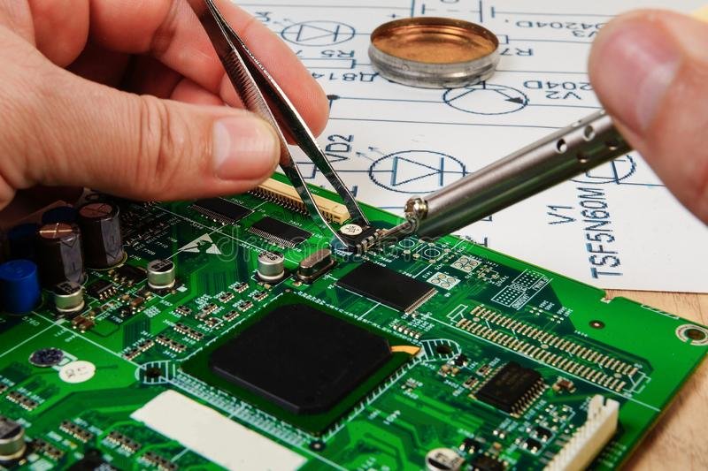
For those interested in the role of test points in circuit layouts, you can learn more about what are test points and how they facilitate troubleshooting and validation.
Component Placement Strategies for Effective Layouts
One of the first steps in any electronics project is component placement. A logical and organized approach ensures optimal signal flow and simplifies assembly. Here are some best practices:
- Group related components: Keep parts that interact closely, such as resistors and capacitors for an integrated circuit, near each other to reduce trace lengths and noise.
- Respect orientation: Align polarized components (like diodes and electrolytic capacitors) consistently to prevent assembly errors and aid inspection.
- Prioritize critical paths: Place timing-sensitive or high-frequency components first, then arrange supporting parts around them.
- Allow for accessibility: Leave space for connectors, test points, and mounting holes to ensure ease of use and testing.
Optimizing Trace Routing and Signal Integrity
Once components are placed, the next challenge is routing traces. Good routing practices are crucial for maintaining signal quality and reducing electromagnetic interference (EMI). Consider these electronics layout tips for trace routing:
- Keep traces short and direct: Shorter traces reduce resistance, inductance, and the risk of signal degradation.
- Use appropriate trace widths: Calculate trace widths based on current requirements to avoid overheating and voltage drops.
- Minimize right angles: Avoid 90-degree bends, as they can cause signal reflections and manufacturing issues. Use 45-degree angles for smoother transitions.
- Separate analog and digital signals: Route sensitive analog traces away from noisy digital lines to prevent interference.
- Implement ground planes: A solid ground plane beneath signal traces helps with noise reduction and provides a low-impedance return path.
For a deeper understanding of how vias impact routing and connectivity, see the article on how vias are made in PCBs.
Thermal Management and Power Distribution
Effective heat dissipation and power delivery are essential for reliable operation, especially in high-power or densely packed designs. Here’s how to address these concerns:
- Distribute power evenly: Use wide traces or dedicated power planes for high-current paths to minimize voltage drops and heating.
- Place heat-generating components carefully: Position power regulators, transistors, and other hot parts near board edges or areas with good airflow.
- Use thermal vias: These help transfer heat from surface-mounted devices to internal or bottom layers, improving dissipation.
- Consider heatsinks and copper pours: For particularly hot components, add heatsinks or increase copper area to spread and dissipate heat efficiently.
Design for Manufacturability and Assembly
A layout that is easy to manufacture and assemble reduces production costs and the likelihood of defects. Keep these points in mind:
- Maintain adequate spacing: Follow the manufacturer’s minimum clearance rules for traces, pads, and components to avoid shorts and solder bridging.
- Standardize footprints: Use industry-standard footprints and pad sizes for components to simplify sourcing and assembly.
- Label clearly: Mark reference designators and polarity indicators on the silkscreen layer for easier assembly and inspection.
- Plan for testing: Add accessible test points and consider how the board will be probed or inspected during quality control. For more on this, explore electronics inspection methods.

Material Selection and Surface Finishes
The choice of materials and surface finishes can influence both performance and durability. Here are some considerations:
- Choose suitable substrates: FR-4 is common for most applications, but high-frequency or high-temperature designs may require specialized materials.
- Pick the right finish: Options like HASL, ENIG, or OSP affect solderability, corrosion resistance, and cost. Match the finish to your assembly process and product lifespan.
- Understand copper thickness: Thicker copper layers handle more current but may require adjustments to trace widths and spacing. For more on this, see copper plating process explained.
Documentation and Review Process
Comprehensive documentation and thorough reviews are crucial for catching errors before production. Here’s how to ensure your layout is ready:
- Maintain up-to-date schematics: Ensure your schematic and layout files are synchronized to avoid mismatches.
- Generate clear assembly drawings: Provide manufacturers with detailed drawings, including component values, orientations, and special instructions.
- Perform design rule checks (DRC): Use your PCB design software’s DRC tools to catch violations of spacing, trace width, and other constraints.
- Conduct peer reviews: Have another engineer review your layout for fresh insights and to catch overlooked issues.
Staying Up to Date with Industry Practices
The field of electronics manufacturing is always evolving. Staying informed about the latest processes and standards helps you design layouts that are robust and future-proof. For a comprehensive overview of how modern electronics are produced, refer to this detailed guide to the electronics manufacturing process.
Frequently Asked Questions
What is the most important factor in a successful electronics layout?
The most critical factor is a balanced approach that considers component placement, trace routing, thermal management, and manufacturability. Prioritizing signal integrity and accessibility for testing also plays a major role in achieving a reliable design.
How can I reduce noise and interference in my PCB design?
To minimize noise, keep analog and digital signals separate, use ground planes, and avoid long parallel traces. Implementing proper decoupling capacitors near power pins and maintaining short, direct connections further helps reduce interference.
Why is documentation so important in electronics layout?
Good documentation ensures that manufacturers, assemblers, and testers can accurately interpret your design. It reduces the risk of errors, speeds up production, and simplifies troubleshooting or future modifications.