


In the world of electronics manufacturing, stencil printing is a fundamental process that directly impacts the quality and reliability of printed circuit boards (PCBs). Understanding how stencil printing works is essential for engineers, technicians, and anyone involved in PCB assembly. This process ensures precise application of solder paste, which is crucial for mounting surface-mount devices (SMDs) onto the board. By mastering the details of stencil printing, manufacturers can minimize defects, improve yields, and produce high-performance electronic products.
Before diving into the technical steps, it’s helpful to recognize how stencil printing fits into the broader context of PCB fabrication. For those interested in related processes, you can explore how PCB drilling works to see how holes are created for through-hole components and vias.
Understanding the Role of Stencil Printing in Electronics Manufacturing
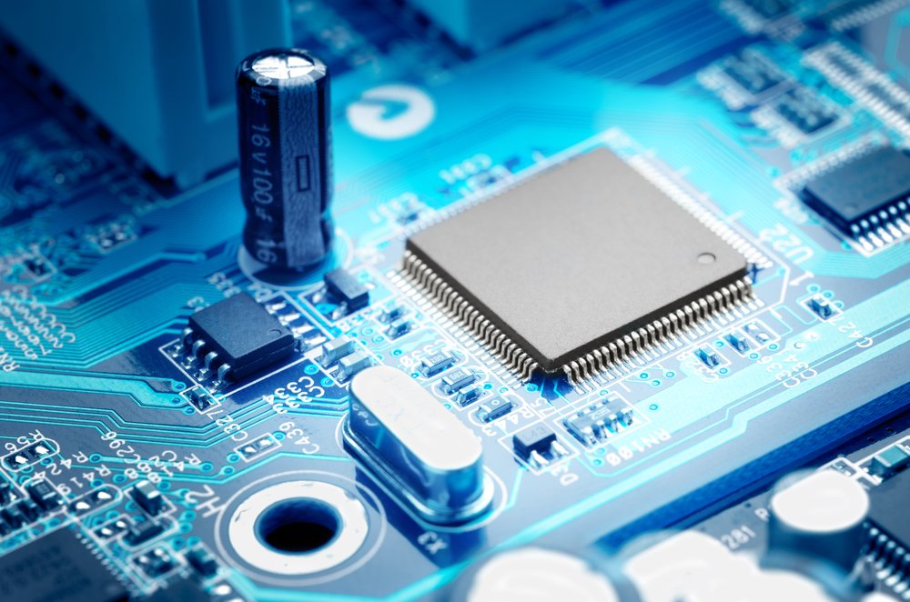
At its core, stencil printing is the method used to deposit solder paste onto specific locations on a PCB. The paste acts as an adhesive and electrical connection point for SMDs. The accuracy and consistency of this step are vital because any misalignment or insufficient paste can lead to soldering defects, such as bridges, tombstoning, or open circuits.
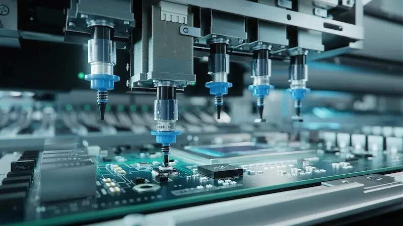
The process uses a thin, laser-cut stencil (typically made from stainless steel) that matches the layout of the PCB’s pads. Solder paste is spread across the stencil using a squeegee, filling the apertures and transferring the paste onto the board below. After the stencil is removed, the PCB is ready for component placement and subsequent reflow soldering.
Key Steps in the Stencil Printing Process
To fully grasp how stencil printing works, it’s helpful to break down the process into its main stages. Each step is designed to ensure precise and repeatable results.
- Stencil Preparation: The stencil is cleaned and inspected for any damage or residue from previous runs. Proper maintenance is crucial for preventing defects.
- Board Alignment: The PCB is positioned under the stencil using alignment systems. Accurate registration ensures that solder paste is applied exactly where needed.
- Solder Paste Application: A squeegee blade moves across the stencil, forcing solder paste through the apertures onto the PCB pads. The pressure and speed of the squeegee are carefully controlled.
- Stencil Separation: The stencil is lifted away from the PCB, leaving solder paste deposits on the pads. The separation speed and angle can affect the quality of the paste deposits.
- Inspection: Automated optical inspection (AOI) or manual checks are performed to verify the consistency and placement of the solder paste.
Equipment and Materials Used in the Process
The effectiveness of stencil printing depends on both the equipment and the materials involved. Here are the primary components:
- Stencil: Usually made of stainless steel, the stencil contains precisely cut apertures that match the PCB layout. The thickness and aperture design influence the volume of solder paste deposited.
- Solder Paste: This is a mixture of powdered solder and flux. The paste’s viscosity and particle size distribution are critical for achieving clean, consistent deposits.
- Printing Machine: Modern stencil printers use automated alignment, pressure control, and cleaning systems to maximize repeatability and minimize errors.
- Squeegee: The blade (metal or polyurethane) spreads the paste across the stencil. The angle and speed of the squeegee affect the filling of apertures.
Factors Affecting Print Quality and Reliability
Achieving optimal results in stencil printing requires careful control of several variables. Here are some of the most important factors:
- Stencil Thickness: Thicker stencils deposit more paste, which may be necessary for larger components but can cause bridging for fine-pitch devices.
- Aperture Design: The shape and size of each aperture must match the pad layout and component requirements.
- Squeegee Pressure and Speed: Too much pressure can damage the stencil or push paste under it, while too little may leave apertures unfilled.
- Pasting Environment: Temperature and humidity can affect paste viscosity and drying, influencing print consistency.
- Stencil Cleaning: Regular cleaning prevents paste buildup and ensures sharp, well-defined deposits.
Common Challenges and Solutions in Stencil Printing
Even with advanced equipment, stencil printing can present challenges that impact the final assembly. Some typical issues include:
- Insufficient Paste: Can lead to weak solder joints or open circuits. Solutions include optimizing stencil thickness and ensuring proper squeegee pressure.
- Excess Paste: May cause solder bridging between pads. Adjusting aperture size and reducing stencil thickness can help.
- Misalignment: Results in misplaced solder deposits. Automated alignment systems and regular calibration are essential.
- Paste Drying: Solder paste exposed to air for too long can dry out, leading to poor transfer. Using paste with appropriate open time and maintaining environmental controls can mitigate this.
Integration with Other PCB Assembly Processes
Stencil printing is just one step in the broader electronics manufacturing workflow. After solder paste application, components are placed onto the PCB, and the assembly moves to the reflow oven for soldering. The quality of the stencil print directly affects the success of these downstream processes.
For a comprehensive overview of the entire electronics manufacturing workflow, you may find this detailed explanation of electronics manufacturing processes useful.
Additionally, understanding related topics such as how multilayer PCBs are made and what is impedance control in PCBs can provide a more complete picture of modern PCB fabrication.
Best Practices for Consistent Results
To ensure high-quality and repeatable results in stencil printing, manufacturers should follow these best practices:
- Regularly inspect and maintain stencils and printing equipment.
- Use solder paste within its recommended shelf life and store it under proper conditions.
- Calibrate alignment systems frequently to prevent misregistration.
- Train operators on correct handling and cleaning procedures.
- Monitor environmental conditions in the printing area.
Frequently Asked Questions
What is the purpose of stencil printing in PCB assembly?
Stencil printing is used to apply solder paste precisely onto the pads of a PCB. This step is critical for ensuring that surface-mount devices are properly attached and electrically connected during the reflow soldering process.
How does stencil thickness affect solder paste deposition?
The thickness of the stencil determines the volume of solder paste deposited onto each pad. Thicker stencils deliver more paste, which is suitable for larger components, while thinner stencils are better for fine-pitch devices to prevent bridging.
What are the main causes of defects in stencil printing?
Common causes include misalignment between the stencil and PCB, improper squeegee pressure, worn or damaged stencils, and environmental factors like humidity or temperature fluctuations. Regular maintenance and process control help minimize these issues.
How often should stencils be cleaned during production?
Stencils should be cleaned regularly, often after every few prints or whenever paste buildup is detected. Automated cleaning systems in modern printers help maintain stencil cleanliness and print quality.
Is stencil printing used for all types of PCBs?
Stencil printing is primarily used for surface-mount technology (SMT) assembly. Through-hole PCBs may not require stencil printing, but hybrid boards with both SMT and through-hole components often use this process for the SMT portion.
For more tips on safe and effective electronics fabrication, consider reviewing these electronics fabrication safety tips.