

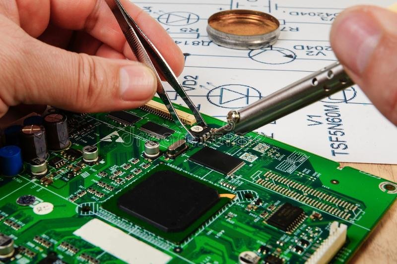
Multilayer printed circuit boards (PCBs) are at the heart of modern electronics, enabling compact, high-performance devices from smartphones to industrial equipment. Understanding how multilayer PCBs are made provides valuable insight into the complexity and precision required in electronics manufacturing. This guide breaks down the essential steps, materials, and quality checks involved in producing these advanced circuit boards.
Before diving into the manufacturing process, it’s helpful to consider the materials and design choices that influence PCB performance. For those interested in substrate selection, you can learn more in our resource on how to choose PCB substrate.

The Basics of Multilayer PCB Construction
At its core, a multilayer PCB consists of several layers of conductive copper and insulating material, stacked and laminated together. These layers allow for complex circuit routing in a compact footprint, supporting high-speed signals and dense component placement. The process of creating these boards involves careful planning, precise fabrication, and rigorous testing.
Design and Material Selection for Complex PCBs
The journey begins with the design phase. Engineers use specialized software to lay out the circuit, specifying the number of layers, trace widths, via locations, and component placements. The choice of substrate—often FR-4, polyimide, or other advanced materials—affects thermal performance, signal integrity, and durability.
Material selection is critical, as it must balance electrical characteristics, mechanical strength, and cost. The copper foil thickness, prepreg (pre-impregnated resin), and core materials are chosen based on the intended application, whether for consumer electronics, automotive systems, or aerospace.
Step-by-Step Process: How Multilayer PCBs Are Manufactured
The manufacturing of multilayer PCBs involves a series of tightly controlled steps. Each stage is vital to ensure the final product meets design specifications and industry standards.
1. Inner Layer Imaging and Etching
The process starts with the inner layers. Copper-clad laminates are cleaned and coated with a light-sensitive photoresist. Using a photomask, the desired circuit pattern is exposed to ultraviolet light, hardening the photoresist where copper should remain.
The unexposed photoresist is washed away, and the exposed copper is etched off, leaving behind the intended circuit traces. After etching, the remaining photoresist is stripped, revealing the finished inner layer circuitry.
2. Layer Alignment and Lamination
Once all inner layers are prepared, they are stacked with layers of prepreg and core material. Precise alignment is crucial; even a slight misalignment can cause electrical failures. The stack is then placed in a heated hydraulic press, where pressure and temperature fuse the layers into a single, solid board.
This lamination process ensures the integrity and insulation between layers, forming the backbone of the multilayer PCB.
3. Drilling and Via Formation
After lamination, holes are drilled through the board to create vias—pathways that connect different layers electrically. High-speed CNC drilling machines ensure accuracy, as via placement is critical for circuit functionality.
The drilled holes are then cleaned and prepared for plating, which will establish the electrical connections between layers.
4. Plating and Outer Layer Imaging
The next step involves plating the drilled holes with a thin layer of copper, forming conductive pathways between layers. The outer layers are then imaged and etched using a process similar to the inner layers, defining the final circuit patterns on the board’s surfaces.
5. Solder Mask, Silkscreen, and Surface Finishing
A protective solder mask is applied to insulate the copper traces and prevent solder bridges during assembly. The silkscreen layer adds component labels, logos, and other markings for assembly and troubleshooting.
Surface finishes, such as HASL (Hot Air Solder Leveling), ENIG (Electroless Nickel Immersion Gold), or OSP (Organic Solderability Preservative), are applied to exposed copper pads to enhance solderability and protect against oxidation.

Quality Control and Testing in PCB Fabrication
Rigorous quality checks are performed throughout the manufacturing process. Automated optical inspection (AOI) systems scan for defects in trace widths, spacing, and alignment. Electrical testing verifies that all connections are correct and that there are no shorts or open circuits.
Additional tests, such as X-ray inspection and cross-section analysis, may be used for high-reliability applications. These steps ensure that the finished product meets the stringent requirements of industries like aerospace, medical, and automotive.
Applications and Benefits of Multilayer PCBs
The ability to stack multiple circuit layers enables designers to create compact, high-density electronic assemblies. Multilayer PCBs are essential in applications requiring high-speed data transfer, reduced electromagnetic interference, and miniaturization.
Their advantages include improved signal integrity, greater design flexibility, and the ability to support complex circuits in a small footprint. These benefits make them indispensable in modern electronics, from consumer gadgets to advanced industrial systems.
Further Reading and Industry Insights
For a deeper dive into the broader electronics manufacturing process, you may find this overview of the electronics manufacturing process helpful. Additionally, understanding related topics such as why PCB traces matter in circuit design can further enhance your knowledge of PCB technology.
Frequently Asked Questions
What materials are commonly used in multilayer PCB manufacturing?
The most common materials include FR-4 (a glass-reinforced epoxy laminate), polyimide, and high-frequency laminates. Copper foil is used for conductive layers, while prepreg and core materials provide insulation and mechanical strength.
How do manufacturers ensure the reliability of multilayer PCBs?
Reliability is achieved through precise manufacturing, strict quality control, and thorough testing. Automated inspections, electrical tests, and sometimes X-ray analysis are used to detect defects and verify correct layer alignment and connectivity.
Why are multilayer PCBs preferred for advanced electronics?
These boards allow for more complex circuit designs, higher component density, and better signal integrity. They are essential for devices that require compact size, high-speed operation, and reduced electromagnetic interference.