

As technology advances, the way electronic components are protected, connected, and integrated has become increasingly important. The choice of electronics packaging types directly affects device performance, reliability, and manufacturability. Whether you’re an engineer, hobbyist, or simply curious about how modern devices are assembled, understanding the main approaches to packaging is essential for anyone involved in electronics design or assembly.
Packaging not only shields delicate components from environmental hazards but also determines how efficiently signals are transmitted and how easily products can be assembled or repaired. If you’re interested in the origins of the parts inside your devices, you may also want to explore how electronics components are made for a deeper understanding of their journey before packaging.
Why Packaging Matters in Electronics
The primary role of packaging in electronics is to protect sensitive circuits and chips from physical damage, moisture, dust, and electromagnetic interference. But its function goes beyond just protection. The right packaging ensures proper electrical connections, supports heat dissipation, and allows for efficient assembly during manufacturing. It can also influence the size, weight, and cost of the final product.
As devices shrink and performance demands grow, the selection of suitable packaging becomes even more critical. Let’s look at the most prevalent forms used in today’s electronics industry.
Through-Hole Packages: Traditional Mounting Solutions
One of the earliest and most recognizable electronics packaging types is the through-hole package. These components have wire leads that are inserted into holes drilled in a printed circuit board (PCB) and then soldered in place. This method provides strong mechanical bonds, making it ideal for components that may face physical stress, such as connectors or large capacitors.
- DIP (Dual In-line Package): Features two parallel rows of pins, commonly used for integrated circuits in early computers and consumer electronics.
- TO (Transistor Outline): Cylindrical or flat packages for transistors and diodes, designed for efficient heat dissipation.
- Axial and Radial Leads: Used for resistors, capacitors, and diodes, with leads extending from either end or from one side.

While through-hole mounting is less common in high-volume, automated assembly today, it remains a staple for prototyping and applications demanding durability.
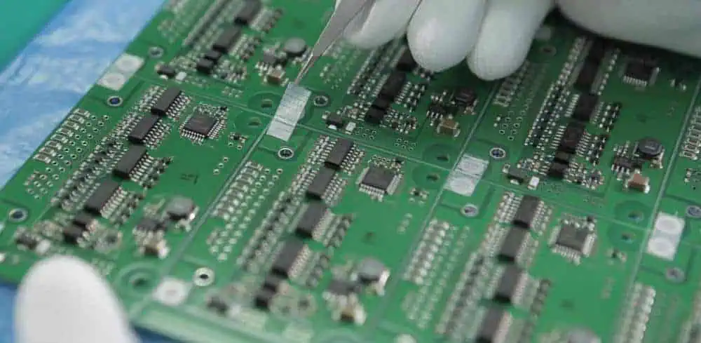
Surface-Mount Technology (SMT): Compact and Efficient
As devices became smaller and more complex, surface-mount packaging emerged as the dominant approach. Unlike through-hole components, SMT parts are mounted directly onto the surface of the PCB, eliminating the need for holes and enabling much higher component densities.
- SOP (Small Outline Package): A compact version of DIP, with gull-wing leads extending from the sides for easy soldering.
- QFP (Quad Flat Package): Integrated circuits with leads on all four sides, ideal for microcontrollers and processors.
- BGA (Ball Grid Array): Uses an array of solder balls on the underside, allowing for even more connections in a small footprint and improved heat dissipation.
- Chip Resistors and Capacitors: Tiny rectangular packages, often just a few millimeters in size, that can be placed automatically by machines.
SMT enables faster assembly, lower costs, and more reliable connections, making it the standard for most modern electronics. For those interested in building their own circuits, resources like a DIY PCB fabrication guide can help you get started with surface-mount projects.
Advanced and Specialized Electronics Packaging Types
As technology continues to evolve, so do the packaging solutions. Advanced packaging addresses challenges like miniaturization, high-speed data transfer, and thermal management. Here are some of the more specialized formats:
- CSP (Chip Scale Package): Nearly the same size as the semiconductor die itself, allowing for extremely compact designs in smartphones and wearables.
- COB (Chip-on-Board): The bare silicon die is mounted directly onto the PCB and wire-bonded, then encapsulated for protection. This method is common in LED modules and some sensors.
- Multi-Chip Modules (MCM): Multiple integrated circuits are packaged together, often with passive components, to create highly integrated solutions for advanced computing and telecommunications.
- System-in-Package (SiP): Combines several chips and passive elements in a single enclosure, enabling complete systems on a single module.
These advanced approaches are crucial for high-performance computing, mobile devices, and IoT applications, where space and efficiency are at a premium.
Key Factors in Choosing a Packaging Solution
Selecting the right packaging for an electronic component involves balancing several considerations:
- Thermal Management: High-power devices require packages that dissipate heat efficiently to prevent failure.
- Electrical Performance: Signal integrity and electromagnetic compatibility can be influenced by the package design and materials.
- Mechanical Strength: Applications subject to vibration or physical stress need robust solutions, often favoring through-hole or reinforced SMT packages.
- Assembly Process: Automated assembly lines favor SMT, while prototyping or repair work may be easier with through-hole parts.
- Cost and Availability: Standardized packages are often more affordable and easier to source than custom or advanced options.
Understanding these factors helps engineers and designers make informed decisions, ensuring both performance and manufacturability.
Testing and Quality Assurance in Electronics Packaging
Regardless of the packaging approach, rigorous testing is essential to ensure reliability. Methods such as visual inspection, X-ray analysis, and electrical testing are commonly used to detect defects like solder bridges, voids, or misalignments. For a detailed look at how these processes work, see the guide on electronics testing methods.
Quality assurance not only improves product reliability but also reduces costly recalls and failures in the field.
Assembly Techniques and Resources
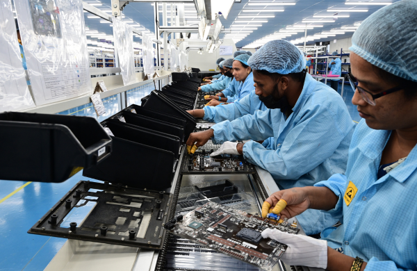
The assembly process varies depending on the packaging type. Manual soldering is still used for prototypes and repairs, while automated pick-and-place machines dominate large-scale production. For those new to electronics, learning about manual assembly techniques for electronics projects can be a valuable starting point.
Additionally, understanding the materials involved in prototyping—such as solder, flux, and PCBs—can help streamline the assembly process. The article on circuit prototyping materials provides a helpful overview for beginners and experienced makers alike.
Frequently Asked Questions
What is the difference between through-hole and surface-mount packaging?
Through-hole packaging involves inserting component leads into holes on a PCB and soldering them in place, providing strong mechanical support. Surface-mount technology, on the other hand, mounts components directly onto the PCB surface, allowing for higher component density and automated assembly.
Why are advanced packaging types like BGA and CSP important?
Advanced formats such as Ball Grid Array (BGA) and Chip Scale Package (CSP) enable greater miniaturization, improved electrical performance, and better heat dissipation. These are essential for modern devices that require high performance in compact spaces, such as smartphones and high-speed computing equipment.
How do I choose the right packaging for my electronics project?
Consider factors like the application’s mechanical and thermal requirements, assembly process, cost, and the need for automated or manual assembly. For most modern designs, surface-mount components offer the best balance of size, cost, and performance, but through-hole parts may be preferable for prototypes or rugged applications.