

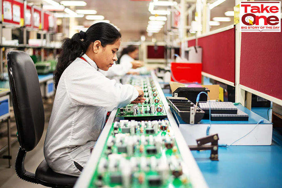
Ensuring the reliability and safety of electronic devices relies heavily on effective electronics testing methods. Whether developing consumer gadgets, industrial equipment, or complex circuit boards, thorough testing is essential to identify defects, verify performance, and maintain quality standards. This guide explores the most widely used approaches for evaluating electronic assemblies, components, and systems, providing a practical overview for engineers, manufacturers, and anyone interested in the field.
Understanding the range of available techniques can help you select the right process for your project, minimize costly failures, and streamline the path from prototype to production. For those interested in the broader context of manufacturing, you may also find value in learning about electronics manufacturing steps and how they integrate with testing protocols.
Why Testing Is Crucial in Electronics Manufacturing
The complexity of modern electronic circuits means that even minor errors can lead to significant malfunctions. By implementing robust testing procedures, manufacturers can detect faults early, reduce product recalls, and ensure compliance with industry standards. Testing also supports continuous improvement, allowing teams to refine designs and processes based on real-world feedback.
In addition to quality assurance, comprehensive testing helps meet regulatory requirements and customer expectations. It is a critical step in the lifecycle of any electronic product, from initial design validation to final inspection before shipment.
Overview of Key Electronics Testing Methods
There are several established approaches to evaluating electronic assemblies and components. Each method serves a unique purpose, and often, multiple techniques are combined for comprehensive coverage. Below are some of the most common strategies used in the industry today.

In-Circuit Testing (ICT)
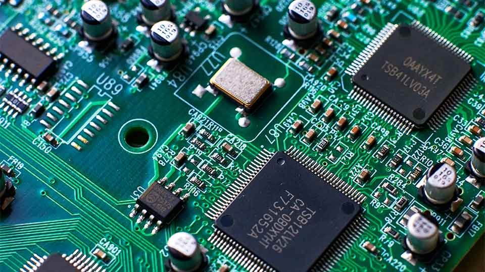
In-circuit testing is a widely used approach for checking assembled printed circuit boards (PCBs). This method uses a bed-of-nails fixture or flying probe to make electrical contact with test points on the board. ICT verifies component placement, solder joint integrity, and basic electrical parameters such as resistance and capacitance.
- Detects manufacturing defects like open circuits, shorts, and incorrect component values
- Automated and fast, making it suitable for high-volume production
- Limited in detecting functional issues or faults in programmable devices
Functional Testing
Functional testing evaluates whether an assembled device or circuit performs its intended operations under simulated or real-world conditions. This method often involves applying power, input signals, and measuring outputs to confirm correct behavior.
- Checks the overall operation of the product, including firmware and software
- Can identify issues missed by ICT, such as timing errors or logic faults
- Typically performed after in-circuit or visual inspection
Automated Optical Inspection (AOI)
Automated optical inspection uses high-resolution cameras and image processing algorithms to examine PCBs for visible defects. AOI systems can quickly spot missing components, misalignments, soldering problems, and other visual anomalies.
- Non-contact and non-destructive
- Effective for catching cosmetic and assembly errors early
- Best used in conjunction with electrical testing for full coverage
Boundary Scan and JTAG Testing
For complex digital circuits, especially those with dense packaging or limited physical access, boundary scan (based on the JTAG standard) provides a powerful way to test interconnections and internal logic. This method uses built-in test circuitry within chips to control and monitor signals, enabling detection of faults that are otherwise hard to reach.
- Ideal for high-density boards and advanced ICs
- Supports programming and debugging as well as testing
- Requires compatible components and test infrastructure
Burn-In and Environmental Stress Testing
To ensure long-term reliability, some products undergo burn-in testing or environmental stress screening. These processes expose devices to elevated temperatures, humidity, vibration, or electrical loads to accelerate aging and reveal latent defects.
- Identifies early-life failures (infant mortality) in components
- Helps guarantee performance under harsh conditions
- May increase testing time and costs but improves confidence in product durability
Additional Inspection and Measurement Techniques
Beyond the primary methods discussed above, several other inspection and measurement tools can enhance the testing process:
- X-ray inspection for detecting hidden solder joint issues, especially in BGAs and multilayer boards
- Flying probe testing for low- to medium-volume runs where fixture costs are prohibitive
- Manual visual inspection for prototype or low-volume assemblies
- Electrical parameter measurement using oscilloscopes, multimeters, and specialized analyzers
Integrating Testing Into the Electronics Production Workflow
Effective implementation of electronics testing methods requires careful planning and integration with the overall manufacturing process. Early-stage design for testability (DFT) can simplify later inspections and reduce costs. For example, including test points, using standard interfaces, and documenting procedures all contribute to smoother testing and troubleshooting.
Testing should be viewed as an ongoing activity, not just a final checkpoint. By incorporating inspection and validation at multiple stages—from incoming materials to final assembly—manufacturers can catch issues sooner and maintain higher quality standards. For more insight into the materials and design considerations that impact testing, explore topics like circuit board materials explained and how to design a PCB.
Emerging Trends and Advanced Approaches
As electronics become more sophisticated, testing technologies continue to evolve. Automation, machine learning, and advanced data analytics are being integrated into inspection systems to improve accuracy and efficiency. For those interested in the latest innovations, a comprehensive overview of the semiconductor fabrication process highlights how state-of-the-art methods are shaping the future of electronics manufacturing.
Additionally, the shift toward miniaturization and higher component densities increases the importance of non-invasive and high-resolution testing techniques. As the industry moves forward, staying informed about new tools and standards will be key to maintaining product quality and competitiveness.
Frequently Asked Questions
What is the difference between in-circuit testing and functional testing?
In-circuit testing checks individual components and connections on a PCB for manufacturing defects, such as shorts or incorrect values, without powering the board. Functional testing, on the other hand, evaluates the complete operation of the assembled device under working conditions, verifying that it performs its intended functions.
Why is automated optical inspection important in electronics production?
Automated optical inspection provides a fast, reliable way to detect visual defects like missing or misaligned components, soldering issues, and other assembly errors. It helps catch problems early in the process, reducing rework and improving overall product quality.
How does boundary scan testing benefit complex circuit boards?
Boundary scan testing, based on the JTAG standard, allows for thorough inspection of interconnections and internal logic in high-density or hard-to-access circuits. It is especially useful for advanced ICs and multilayer boards, enabling fault detection, programming, and debugging without physical probes.