

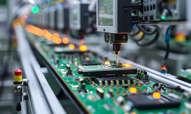
Printed circuit boards (PCBs) are the backbone of nearly every electronic device, from simple gadgets to complex computers. For those interested in electronics, learning how to create your own PCBs is a valuable skill. This DIY PCB fabrication guide is designed to help beginners understand the essential steps, tools, and tips for making circuit boards at home. Whether you want to prototype a new idea or gain hands-on experience, this article will walk you through the process in clear, practical terms.
Before diving into the fabrication process, it’s helpful to understand the basics of PCB design and materials. If you’re new to this area, you might want to explore topics like how to design a PCB or get familiar with what is a Gerber file—the standard format for PCB manufacturing.
Understanding the Basics of Home PCB Production
At its core, a PCB is a flat board made from insulating material, usually fiberglass, with conductive copper traces that connect electronic components. Creating a board at home involves transferring a circuit pattern onto copper-clad material, etching away unwanted copper, and then drilling holes for components.
There are several methods for making PCBs yourself, but most beginners start with the toner transfer or photoresist technique. These approaches are accessible, require minimal investment, and produce reliable results for simple to moderately complex circuits.
Essential Tools and Materials for a DIY PCB Fabrication Project
Before starting your first board, gather the following tools and materials:
- Copper-clad board (single or double-sided, depending on your design)
- Laser printer (for toner transfer method) or transparency film (for photoresist method)
- Etching solution (ferric chloride is common, but alternatives like ammonium persulfate are available)
- Iron or laminator (for transferring toner to the board)
- Drill with small bits (0.8–1.0 mm) for component holes
- Protective gloves and goggles (etchants are hazardous)
- Plastic or glass container for etching
- PCB layout software for designing your circuit (many free options exist)
For a deeper dive into the materials used in circuit boards, you can read about circuit board materials explained to understand how each component affects performance and durability.
Step-by-Step: Creating Your First PCB at Home
1. Designing the Circuit Layout
Start by drawing your schematic using PCB design software. Once your schematic is complete, convert it to a board layout, arranging the traces and pads for your components. Export your design as a mirrored image (for toner transfer) or as a negative (for photoresist).
If you’re unsure about the design process, many resources are available online, such as this comprehensive PCB basics tutorial that covers layout, layers, and best practices.
2. Transferring the Design to the Board
For the toner transfer method, print your PCB layout onto glossy paper using a laser printer. Place the paper face-down on the copper board and use a hot iron or laminator to transfer the toner. Once cooled, soak the board in water and gently remove the paper, leaving the toner as a resist.
If using the photoresist method, print your design on transparency film and expose the coated board to UV light. Develop the board in the appropriate solution to reveal the pattern.
3. Etching Away Unwanted Copper
Submerge the prepared board in your etching solution, agitating gently. The exposed copper will dissolve, leaving only the traces protected by toner or resist. This step can take anywhere from 10 to 45 minutes, depending on the etchant and temperature.
Once etching is complete, rinse the board thoroughly with water. Remove the toner or resist using acetone or a suitable solvent, revealing the copper traces.
4. Drilling and Finishing Touches
Use a small drill to create holes for through-hole components. Clean the board with isopropyl alcohol to remove any residue. For better solderability, you can apply a thin layer of flux or tin the traces with solder.
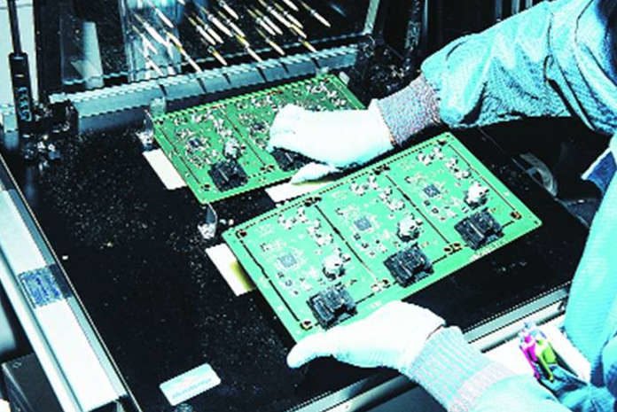
At this stage, your board is ready for component placement and soldering. If you’re interested in learning more about assembly, the article on how reflow soldering works provides insight into modern soldering techniques.
Common Challenges and Troubleshooting Tips
Beginners often encounter issues such as incomplete toner transfer, under-etched or over-etched boards, and misaligned holes. Here are some practical tips to help you avoid common pitfalls:
- Ensure your copper board is clean and free of oils before transferring the design.
- Use consistent, firm pressure and adequate heat during toner transfer.
- Monitor the etching process closely to prevent over-etching, which can thin or break traces.
- Double-check your drill bit size and alignment before drilling holes.
- Work in a well-ventilated area and always wear protective gear when handling chemicals.
Expanding Your Skills in PCB Prototyping
Once you’re comfortable with single-layer boards, you can experiment with double-sided designs, surface-mount components, and more advanced fabrication techniques. Understanding the DIY PCB fabrication guide principles will help you build confidence and tackle more complex electronics projects.
For a broader perspective on the entire process, including assembly and testing, see the overview on electronics manufacturing steps.
Frequently Asked Questions
What is the easiest method for making PCBs at home?
The toner transfer method is widely considered the most accessible for beginners. It requires only a laser printer, glossy paper, an iron, and basic etching supplies. This approach is suitable for simple, single-layer designs.
How do I avoid under-etching or over-etching my board?
Carefully monitor the etching process and agitate the solution gently. Remove the board as soon as the unwanted copper is gone. Using fresh etchant and maintaining the recommended temperature will also help achieve clean results.
Can I make double-sided PCBs at home?
Yes, but it requires precise alignment of the top and bottom layers during the transfer process. Double-sided boards are more challenging but achievable with patience and careful technique.
What safety precautions should I take?
Always wear gloves and goggles when handling etching chemicals. Work in a well-ventilated area, and dispose of used chemicals according to local regulations.
Conclusion
Learning to fabricate your own circuit boards is a rewarding skill that opens up new possibilities in electronics. By following this DIY PCB fabrication guide and practicing safe, careful techniques, you’ll be able to prototype and build custom circuits for a wide range of projects. As you gain experience, you can explore more advanced methods and materials, further expanding your capabilities in the world of electronics.