

Printed circuit boards (PCBs) are at the heart of nearly every electronic device, from smartphones to industrial machinery. Understanding the basics of how these essential components are made is crucial for engineers, designers, and anyone interested in electronics manufacturing. This intro to PCB fabrication covers the essential steps, materials, and best practices involved in transforming a circuit design into a physical, functional board.
Whether you are a hobbyist starting your first electronics project or a professional seeking to optimize your workflow, a solid grasp of PCB manufacturing processes can help you make informed decisions, avoid common pitfalls, and ensure reliable performance. For those interested in the broader context of hardware development, exploring topics like hardware design trends and innovations can provide valuable insights into how PCB technology fits within the evolving landscape of electronics.
Understanding the PCB Manufacturing Process
The journey from schematic to finished board involves several precise and interconnected steps. Each stage in the PCB fabrication process must be carefully executed to ensure the final product meets electrical, mechanical, and reliability requirements. Below, we outline the main phases you’ll encounter when producing a PCB.
Design and Layout: The Foundation of Every Board
Every successful project begins with a well-thought-out design. Using electronic design automation (EDA) tools, engineers create a schematic that defines the circuit’s electrical connections. This schematic is then translated into a PCB layout, specifying the placement of components and the routing of copper traces.
- Component placement affects signal integrity and manufacturability.
- Trace routing must consider current capacity, signal speed, and interference.
- Design rules ensure clearances and dimensions meet manufacturing capabilities.
Before moving to production, it’s common to perform design verification and validation to catch errors early. If you’re interested in how these processes differ, see the detailed comparison in design verification vs validation in hardware.
Material Selection and Preparation
The choice of materials significantly impacts the board’s performance and cost. Most PCBs use a fiberglass-reinforced epoxy laminate (FR-4) as the base, with copper foil laminated on one or both sides. For high-frequency or specialized applications, alternative substrates like polyimide or ceramic may be used.
- Substrate: Provides mechanical support and electrical insulation.
- Copper foil: Forms the conductive pathways for signals and power.
- Solder mask: Protects copper traces and prevents solder bridging.
- Silkscreen: Adds component labels and markings for assembly.
Step-by-Step Guide to PCB Fabrication
The actual manufacturing of a PCB involves transforming the digital layout into a tangible board. Here’s a closer look at the key steps in the intro to PCB fabrication process:
Imaging and Etching: Creating the Circuit Pattern
The first major step is transferring the circuit pattern onto the copper-clad laminate. This is typically done using a photolithographic process:
- Photoresist application: A light-sensitive material is applied to the copper surface.
- Exposure: The board is exposed to ultraviolet light through a mask that defines the circuit pattern.
- Development: The unexposed photoresist is washed away, revealing areas of copper to be etched.
- Etching: Chemical solutions remove the unwanted copper, leaving only the desired traces.

Drilling and Plating: Establishing Connections
After the circuit pattern is defined, holes are drilled for component leads and vias (connections between layers). For multilayer boards, these holes are then plated with copper to ensure electrical continuity.
- Precision drilling is essential for component fit and electrical performance.
- Plated through-holes connect different layers within the board stack-up.
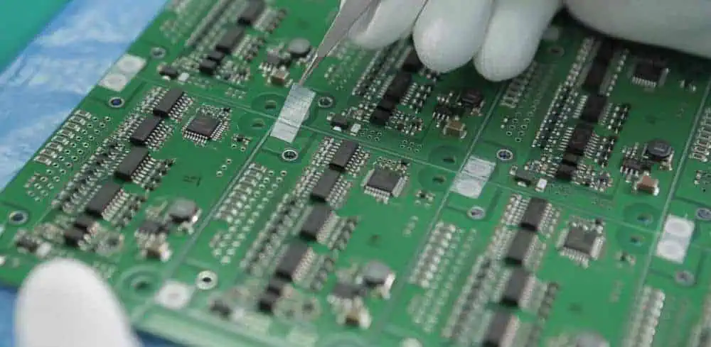
Applying Solder Mask and Silkscreen
The next stage involves coating the board with a solder mask, which insulates and protects the copper traces while exposing only the pads where components will be soldered. A silkscreen layer is then printed to add reference designators, logos, and other helpful markings.
Surface Finishing and Quality Control
To ensure reliable soldering and long-term performance, exposed copper pads are coated with a surface finish such as HASL (Hot Air Solder Leveling), ENIG (Electroless Nickel Immersion Gold), or OSP (Organic Solderability Preservative). The finished boards undergo electrical testing and visual inspection to catch defects before assembly.
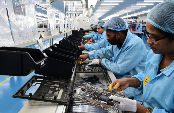
PCB Assembly: From Bare Board to Working Device
Once the bare boards are fabricated, the next step is populating them with electronic components. This process, known as PCB assembly, can be performed manually for prototypes or small batches, or by automated machines for larger production runs.
For those new to electronics manufacturing, learning about manual PCB assembly techniques can be a valuable starting point. Manual assembly is often used for prototyping, repair, or low-volume production, while automated surface-mount technology (SMT) lines are preferred for high-speed, high-volume output.
- Component placement can be done by hand or with pick-and-place machines.
- Soldering methods include hand soldering, wave soldering, and reflow soldering.
- Inspection and testing ensure that the assembled boards function as intended.
Integrating assembly considerations early in the design phase can help streamline manufacturing and reduce costly rework. For a comprehensive overview of the entire development cycle, see the hardware engineering project workflow guide.
Best Practices and Tips for Successful PCB Projects
Achieving high-quality results in PCB manufacturing requires attention to detail and proactive planning. Here are some practical recommendations to help ensure your projects run smoothly:
- Follow design for manufacturability (DFM) guidelines to minimize production issues and costs.
- Communicate clearly with your fabrication partner about specifications, tolerances, and deadlines.
- Prototype and test early to catch errors before committing to full-scale production. Early feedback can be invaluable—learn more about the importance of early prototyping feedback.
- Document everything, including design files, bills of materials, and assembly instructions, to support troubleshooting and future revisions.
- Stay updated on industry trends and emerging technologies to leverage new materials, processes, and tools.
Common Challenges in PCB Fabrication and How to Overcome Them
Even experienced engineers can encounter obstacles during the board manufacturing process. Some frequent challenges include:
- Signal integrity issues caused by poor layout or inadequate grounding.
- Manufacturing defects such as open circuits, shorts, or misaligned layers.
- Component sourcing delays impacting assembly timelines.
- Thermal management problems leading to overheating or reduced reliability.
Addressing these issues requires a combination of solid design practices, thorough testing, and close collaboration with manufacturing partners. For troubleshooting tips and strategies, refer to the guide on how to troubleshoot hardware prototypes.
Frequently Asked Questions
What is the difference between single-layer and multilayer PCBs?
Single-layer boards have components and traces on only one side, making them suitable for simple circuits. Multilayer PCBs stack multiple layers of copper and insulating material, allowing for more complex designs, higher component density, and improved signal integrity.
How long does it take to fabricate a PCB?
The turnaround time depends on the complexity, size, and quantity of boards. Simple prototypes can often be produced within a few days, while more complex or high-volume orders may take several weeks. Early communication with your manufacturer can help set realistic expectations.
What are the most common causes of PCB failure?
Typical causes include design errors, manufacturing defects, poor soldering, and environmental factors like moisture or excessive heat. Rigorous testing and quality control throughout the process help minimize these risks.
Conclusion
Gaining a strong understanding of the intro to PCB fabrication process empowers you to design, produce, and assemble reliable electronic products. By following best practices, staying informed about industry developments, and maintaining open communication with your manufacturing partners, you can navigate the challenges of PCB production with confidence and efficiency.