

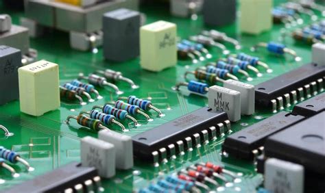
The Printed Circuit Board (PCB) is the backbone of any electronic device. It connects and helps communicate between different hardware components. But did you know that the layout of a PCB plays a crucial role in the overall performance of the hardware? In this article, we delve into the significance of PCB layout in hardware design.

Before we proceed, it might be beneficial to understand the difference between hardware emulation and simulation, as it can also impact the design process.
Understanding the Role of PCB Layout
The design of a PCB layout is a critical aspect of hardware design. It involves placing and routing components on the PCB in a way that optimizes electrical performance and reliability. The layout can affect signal integrity, power distribution, electromagnetic compatibility, and even the manufacturability of the board.
Impacts of Poor PCB Layout
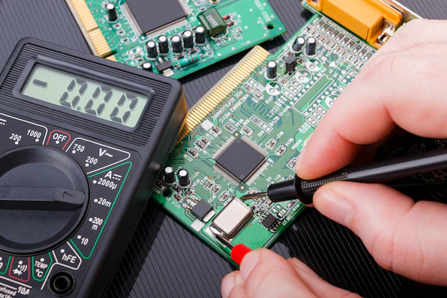
An inefficient PCB layout can lead to a plethora of problems. It can cause signal interference, leading to poor performance or even failure of the device. Moreover, it can also lead to overheating, which can damage components and reduce the lifespan of the device.
Benefits of a Good PCB Layout
A well-designed PCB layout can significantly improve the performance and reliability of the hardware. It ensures optimal signal integrity, reduces power consumption, and enhances the durability of the device. Additionally, it can also simplify the manufacturing process and reduce costs.
Conclusion
In conclusion, the layout of a PCB is a critical factor that determines the success of a hardware design. It’s not just about placing components on a board; it’s about optimizing the layout for maximum performance and reliability. To learn more about hardware prototyping, you can visit this descriptive guide on hardware prototyping for user experience.
Author: Ethan Carter
Publication Date: 2025-10-30